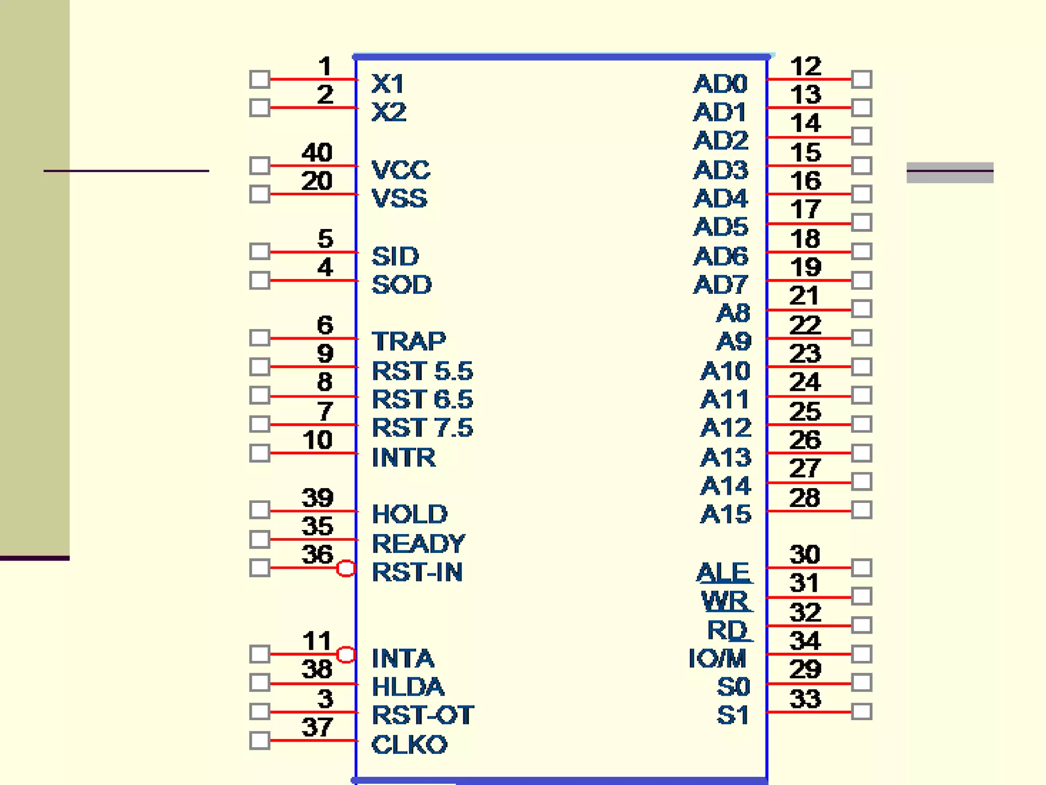
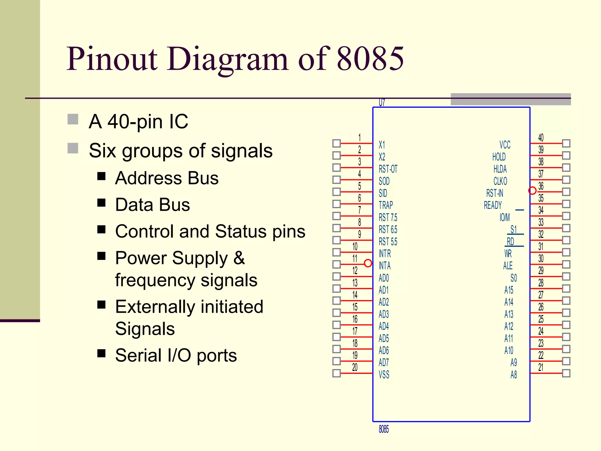
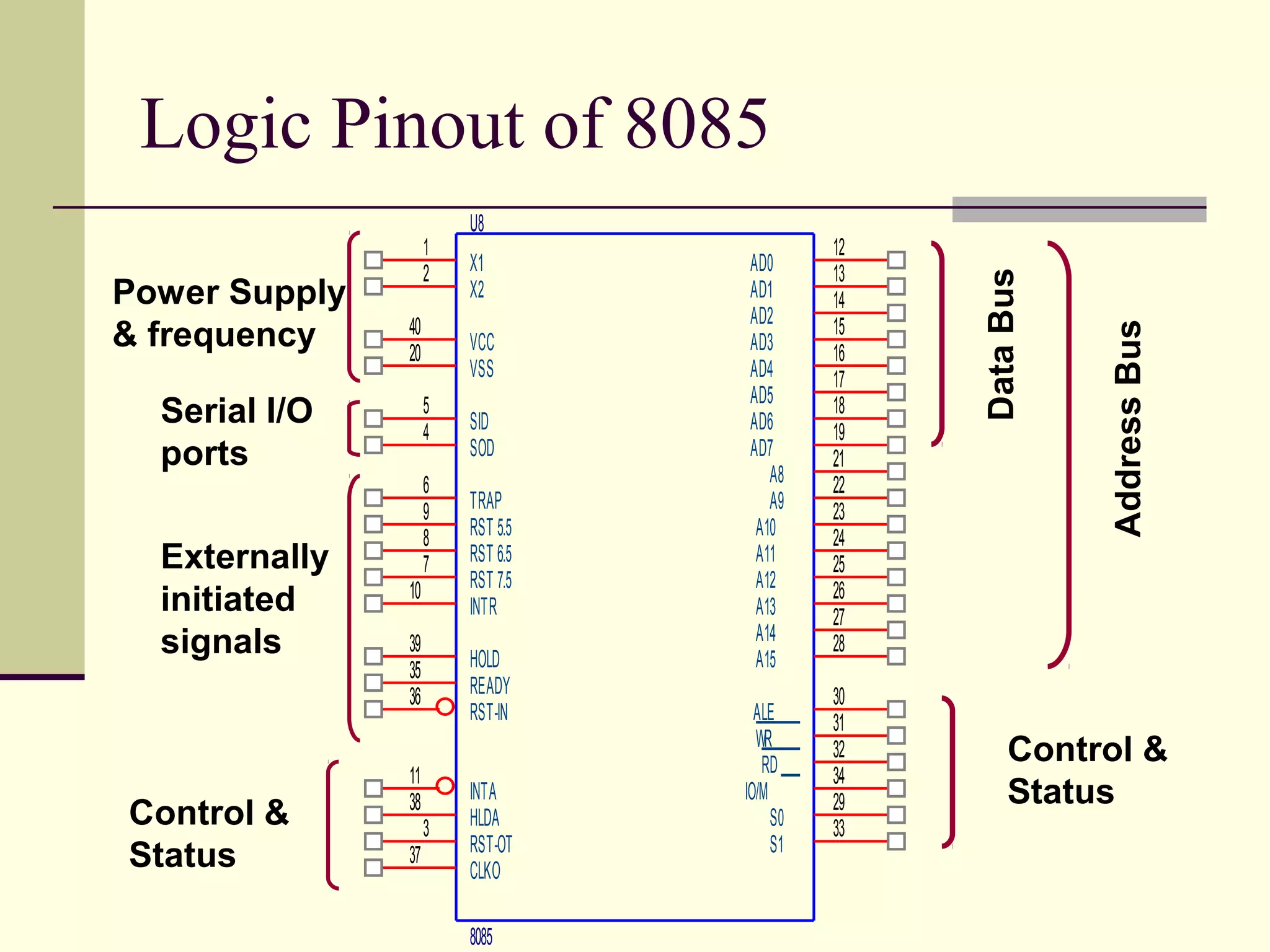
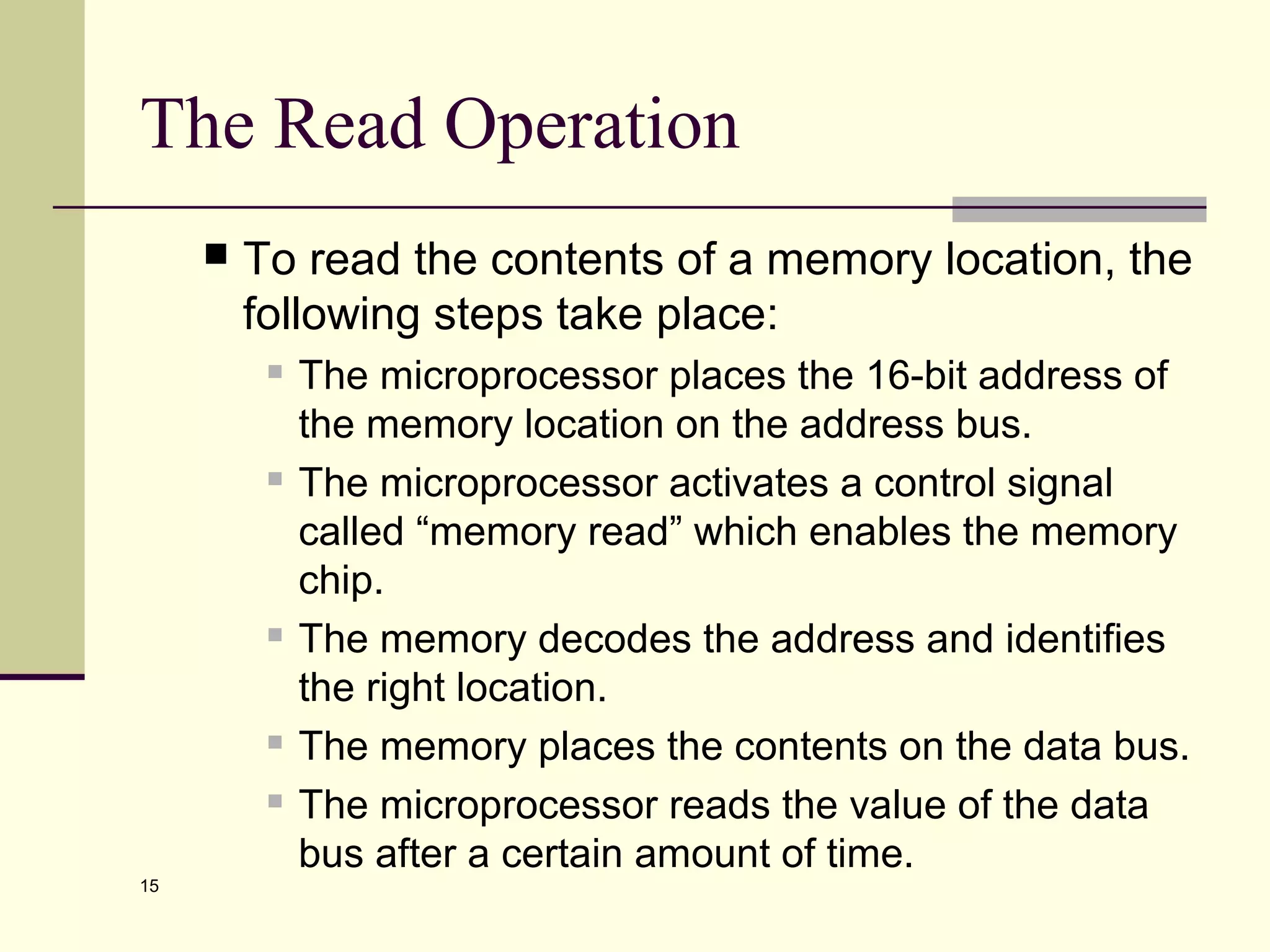
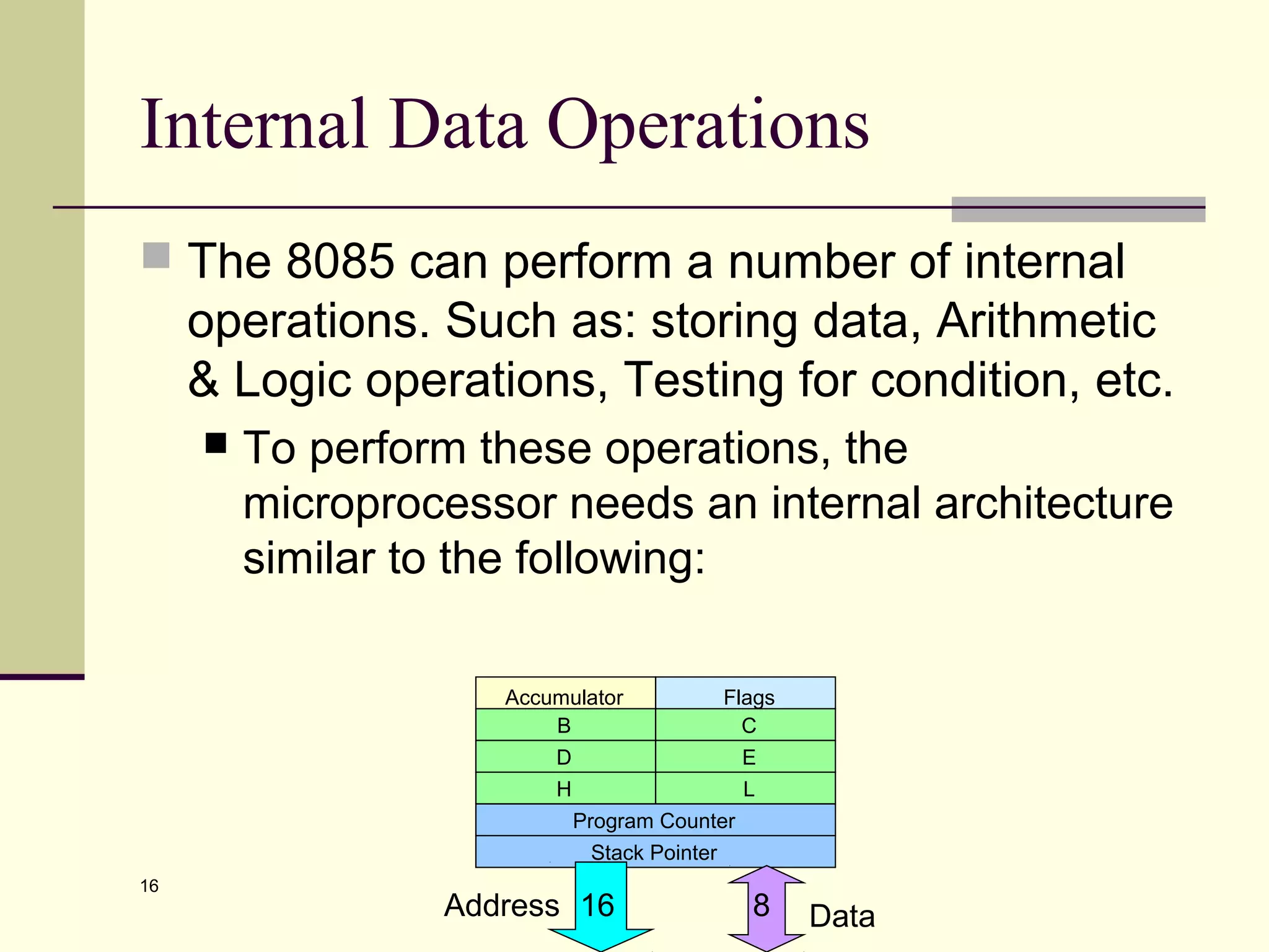
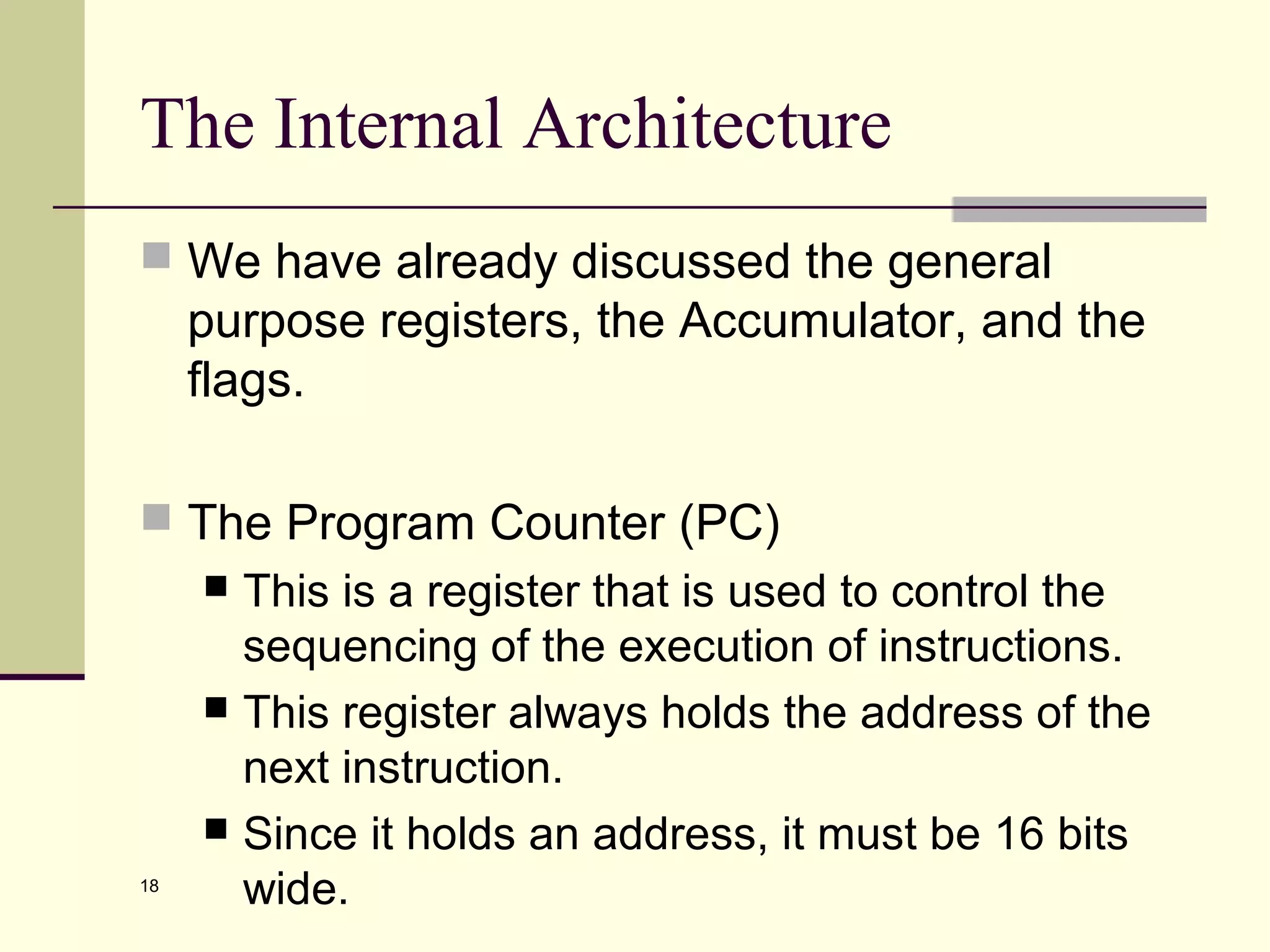
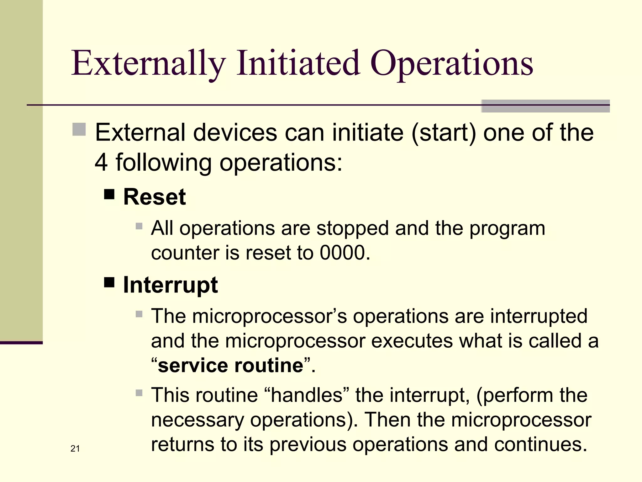
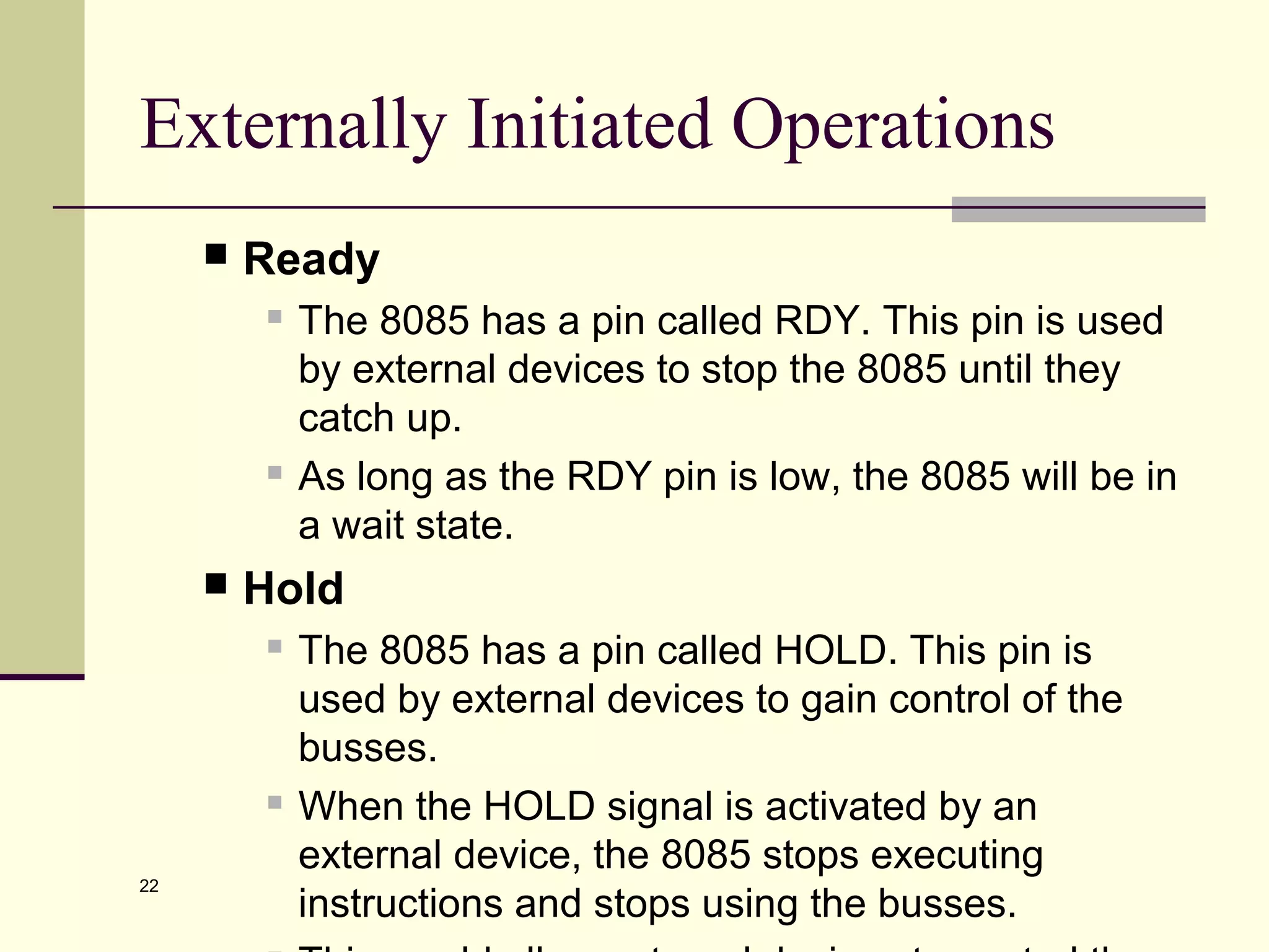
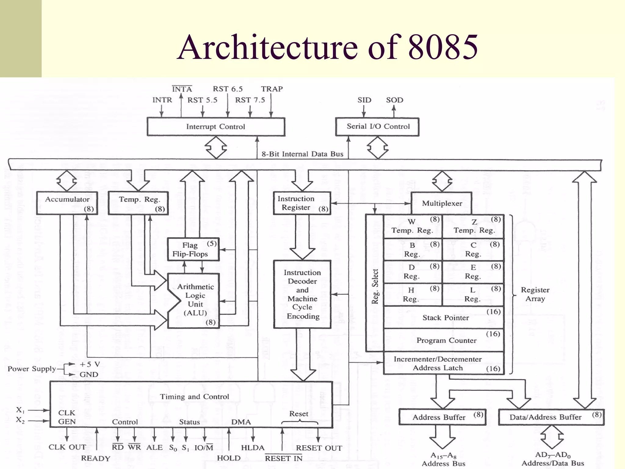
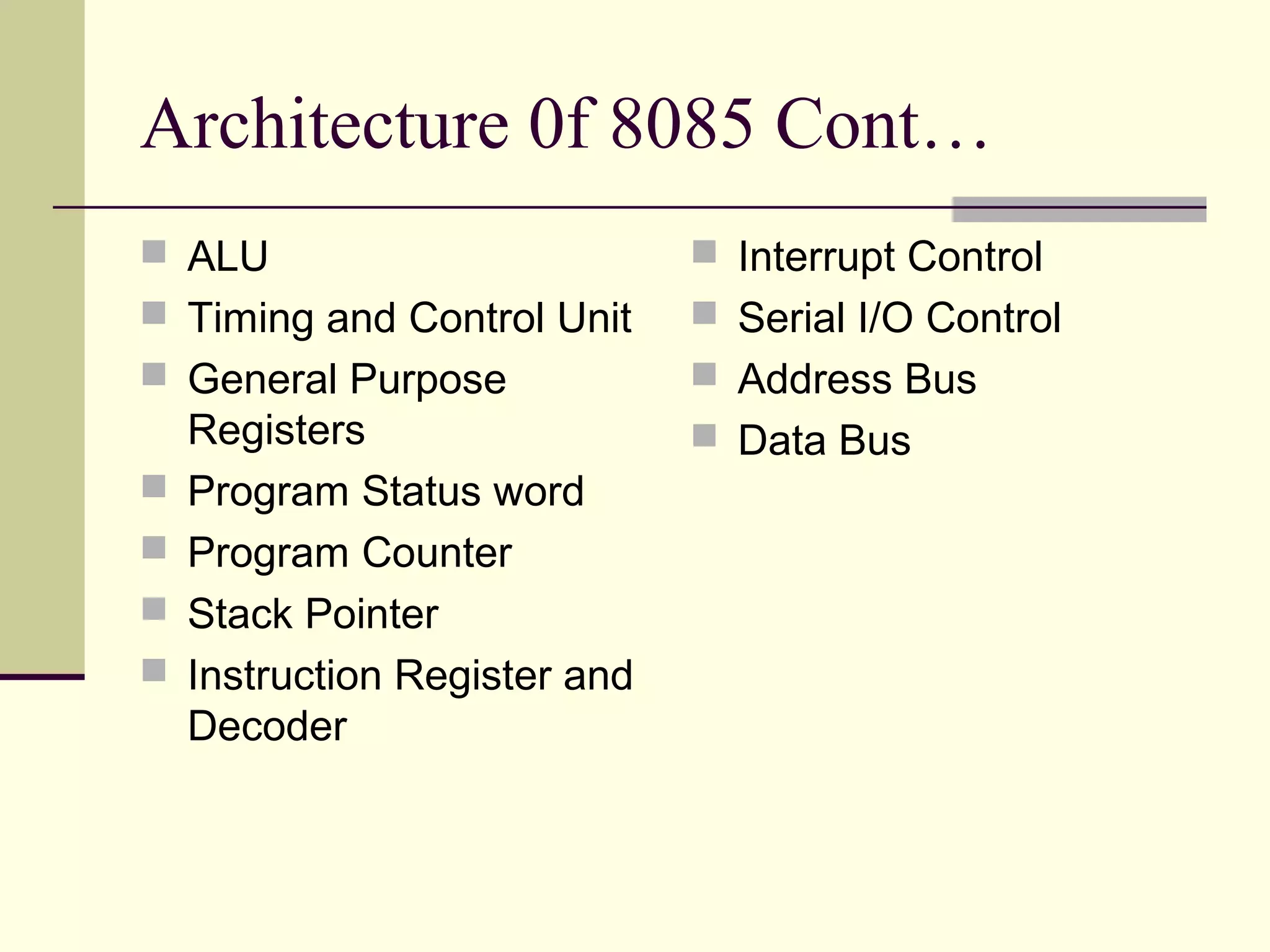
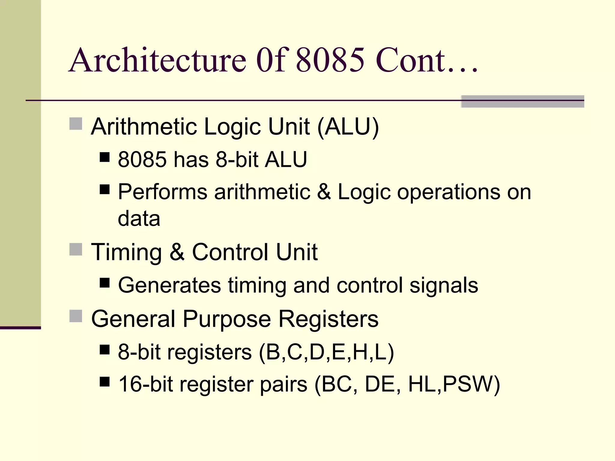
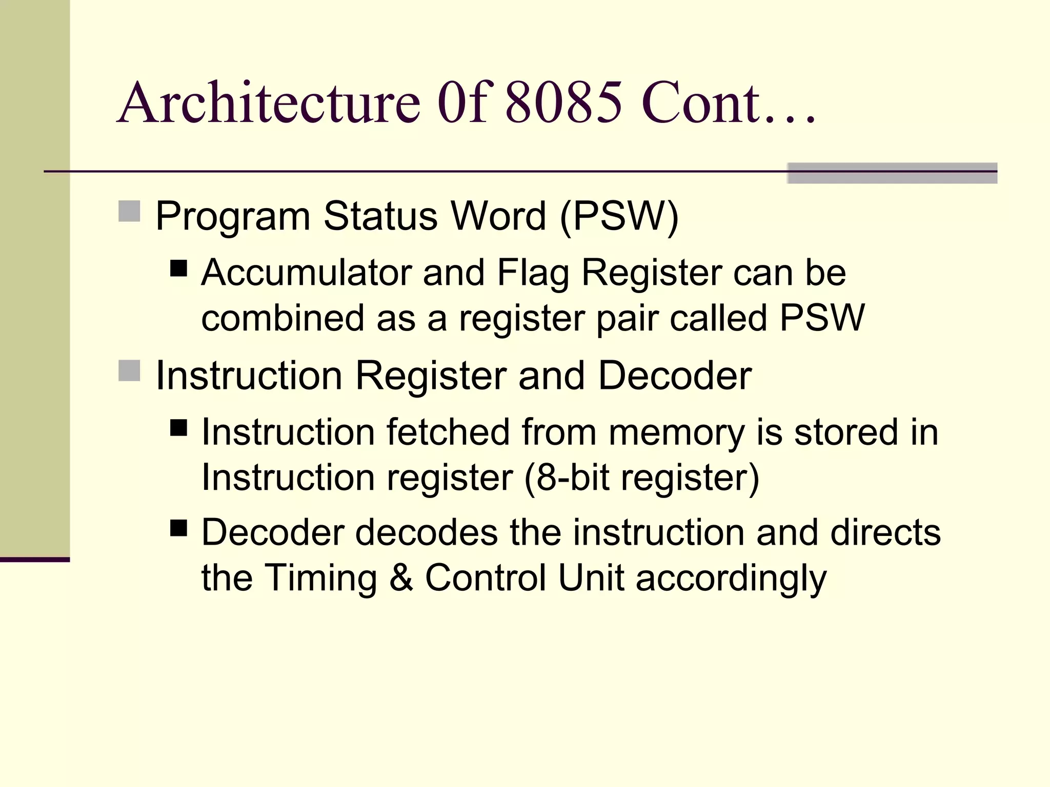
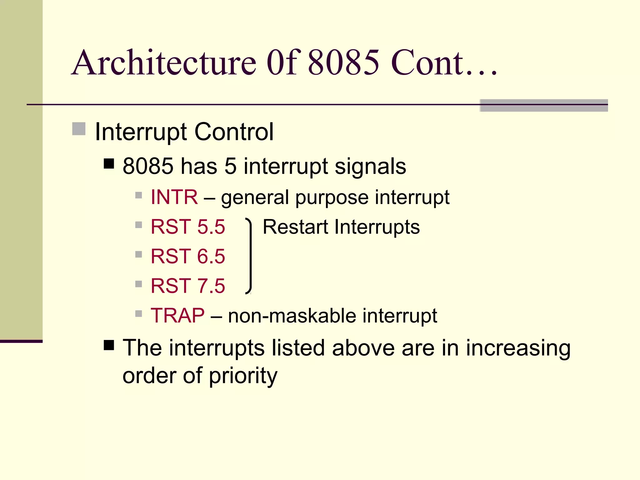
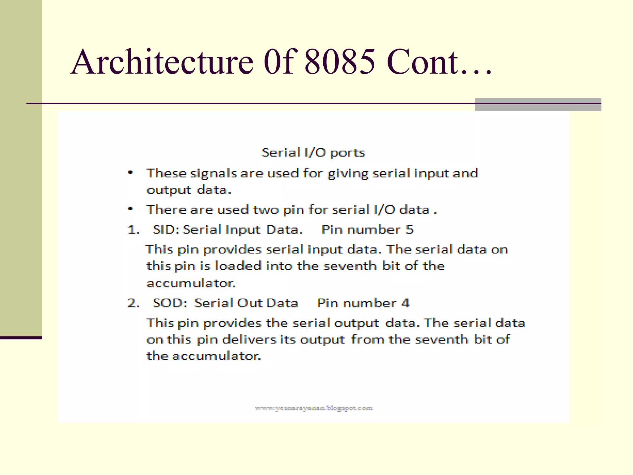
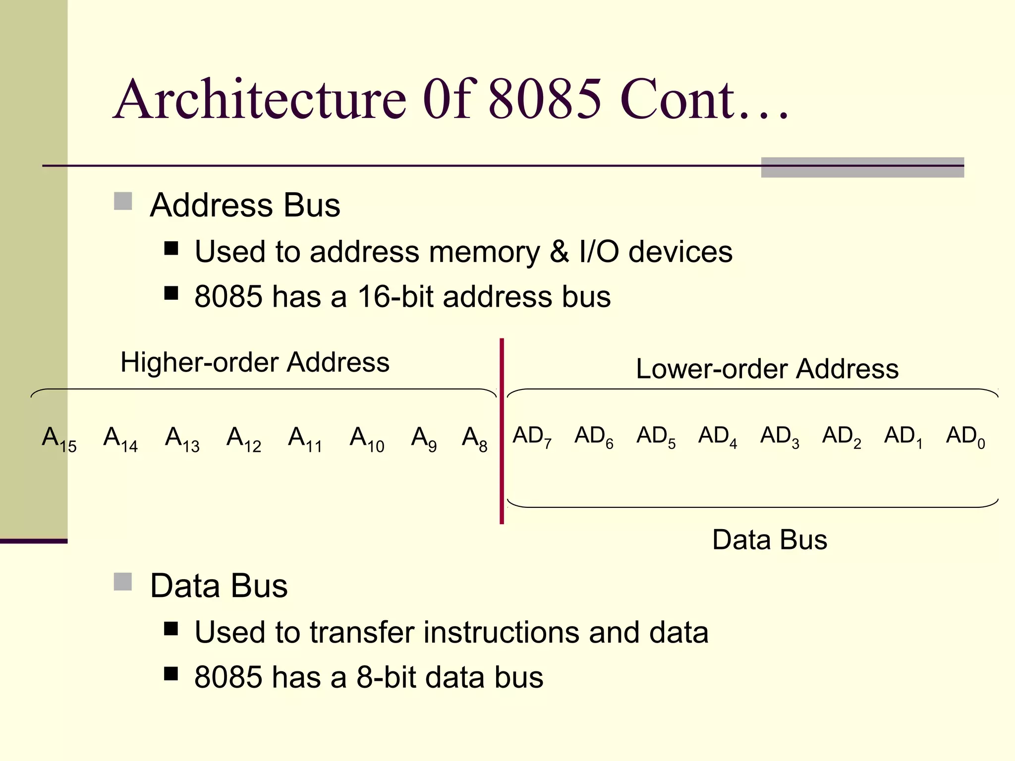
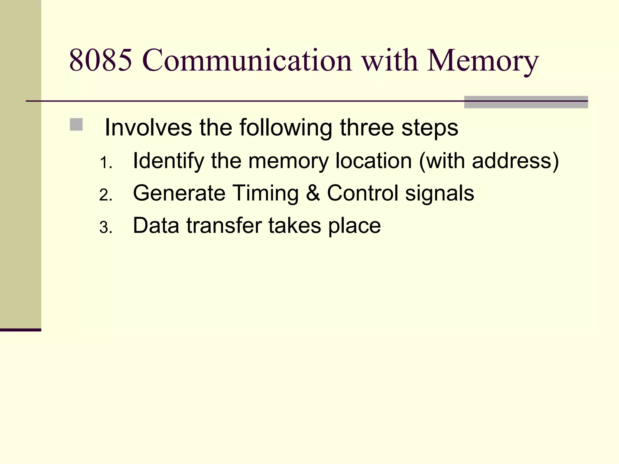
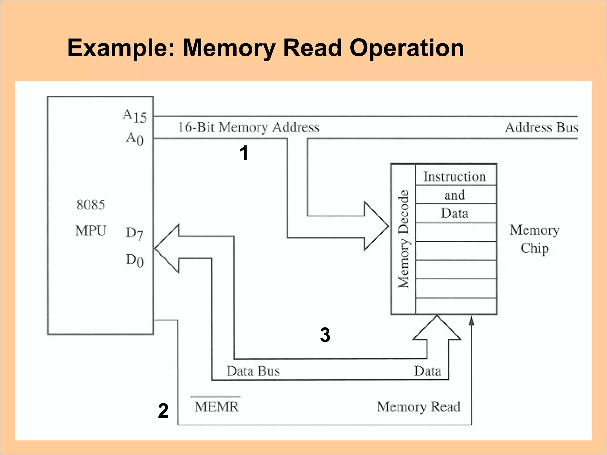
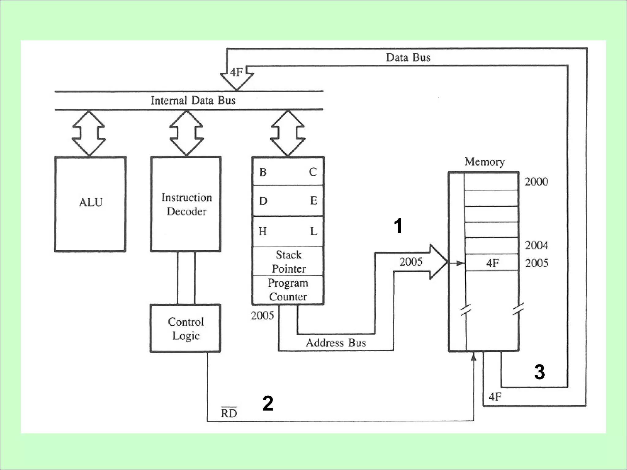
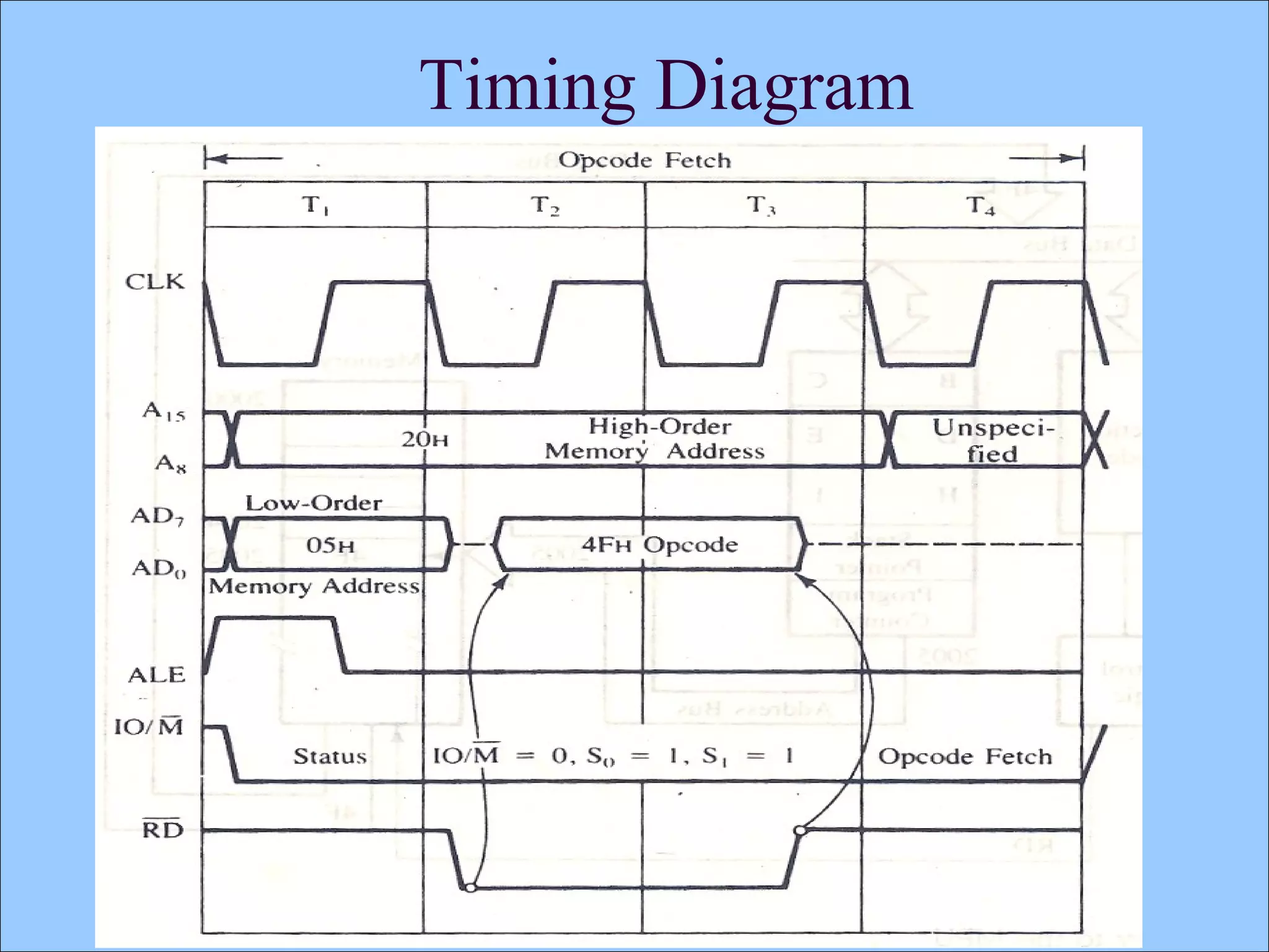
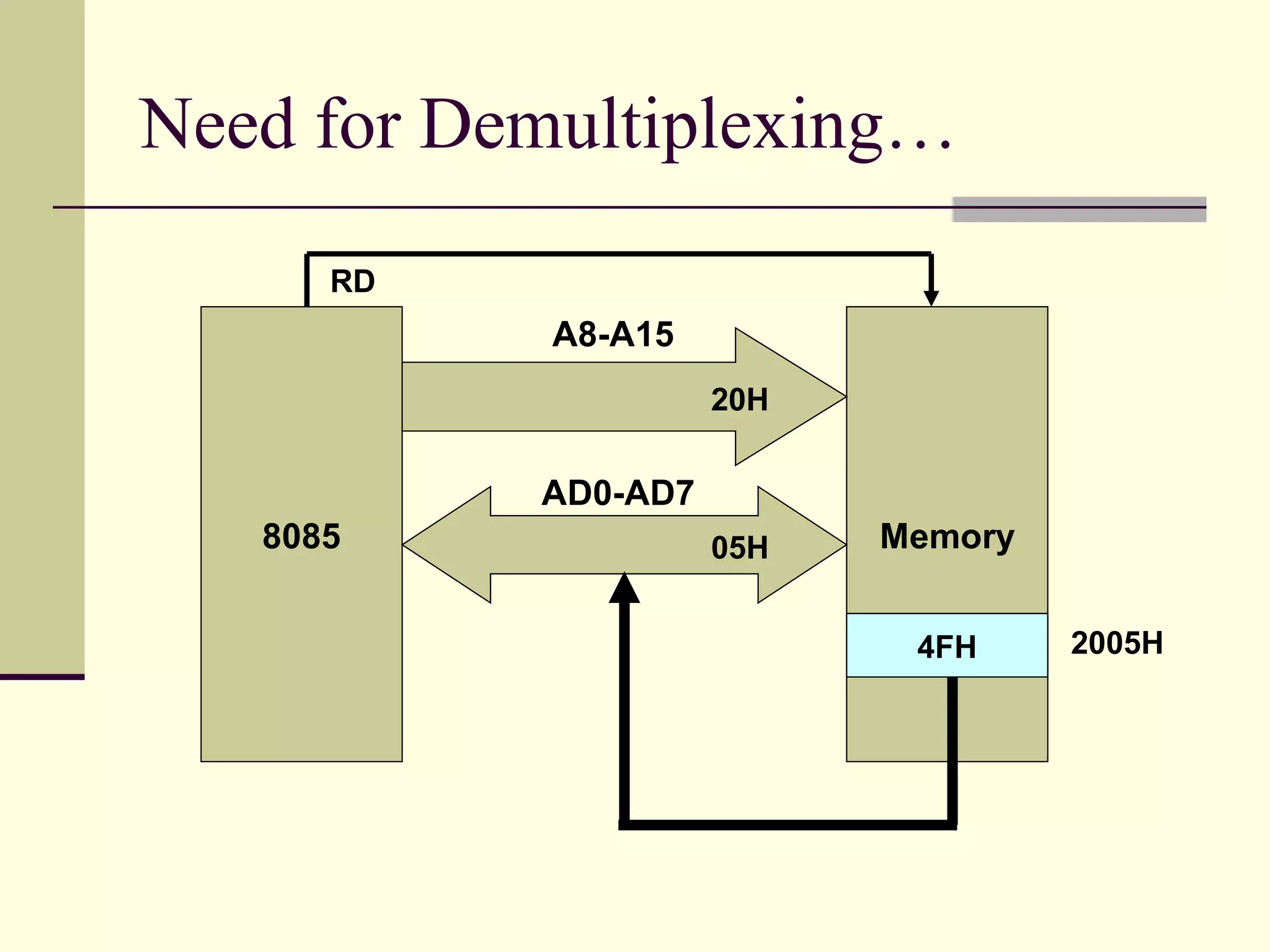
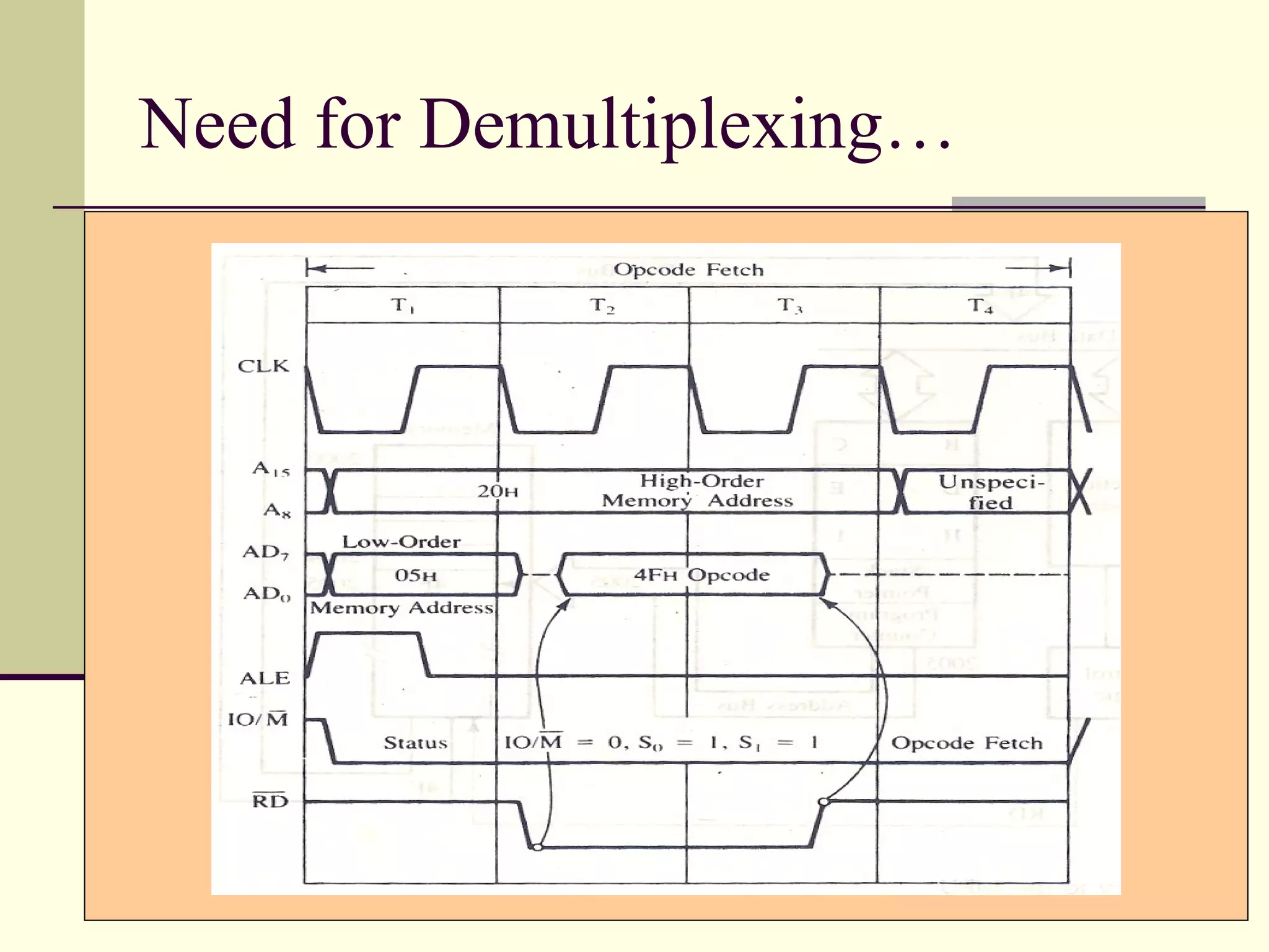
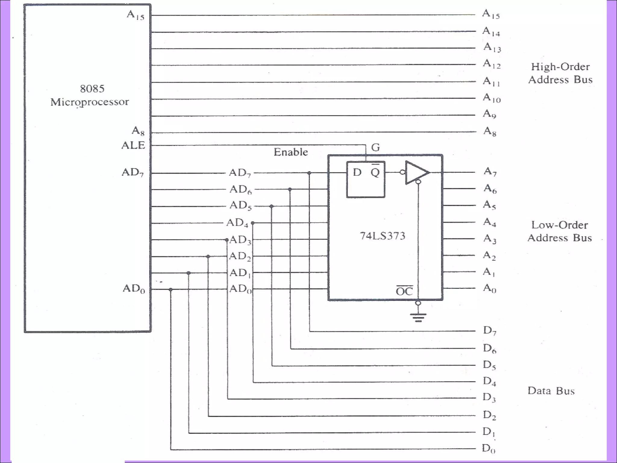
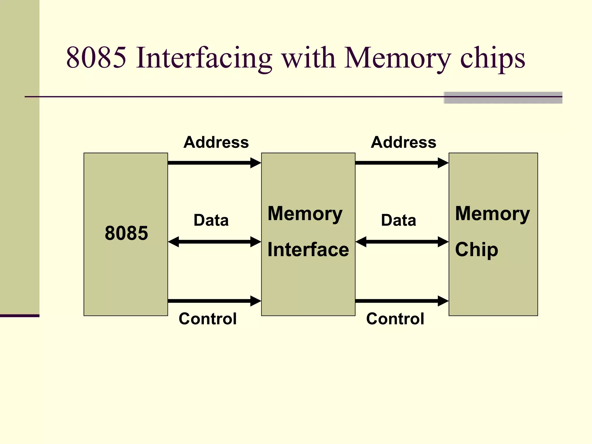
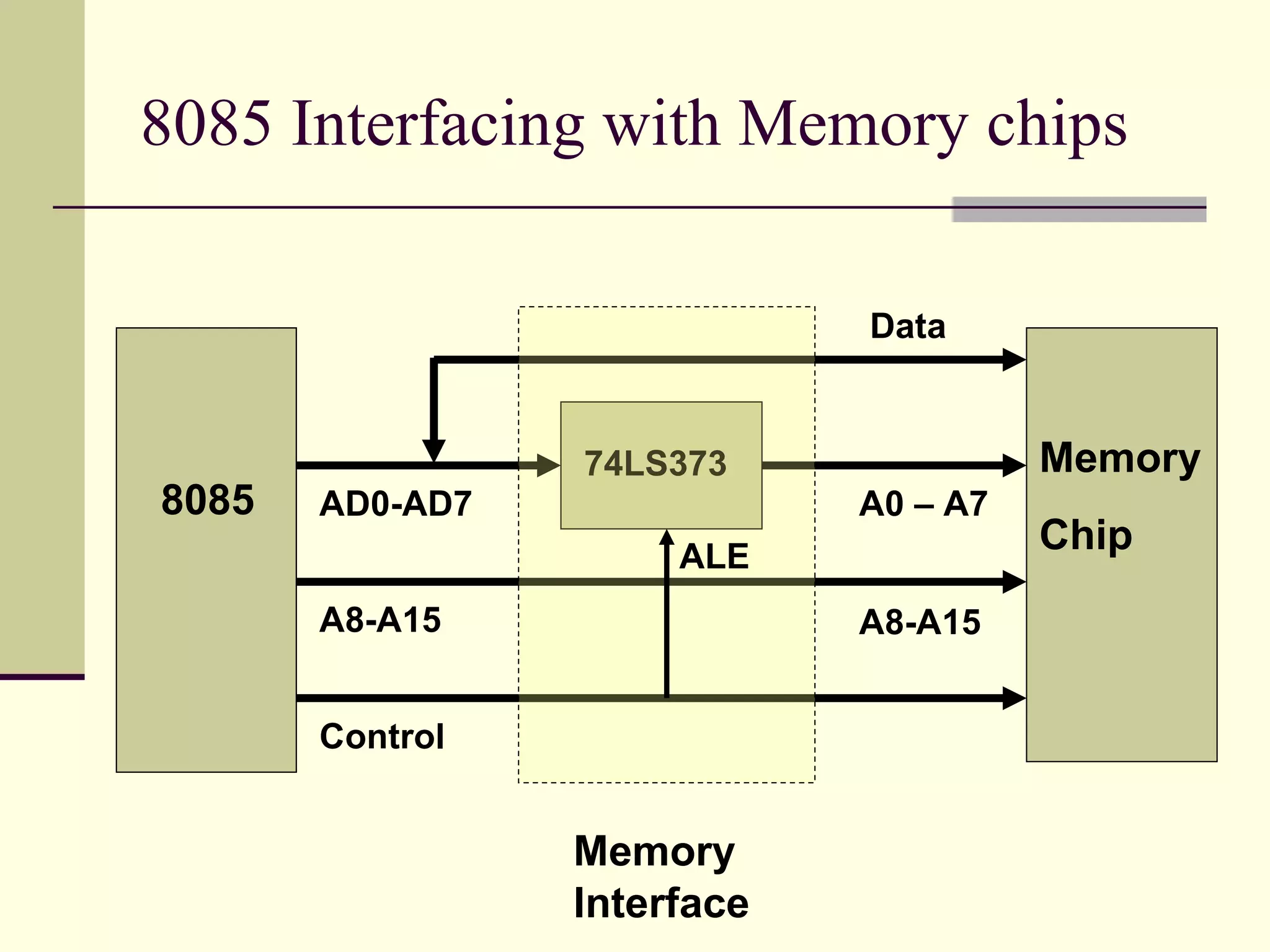
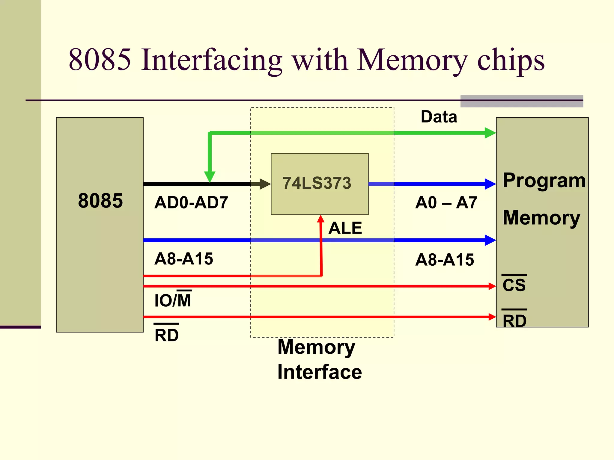
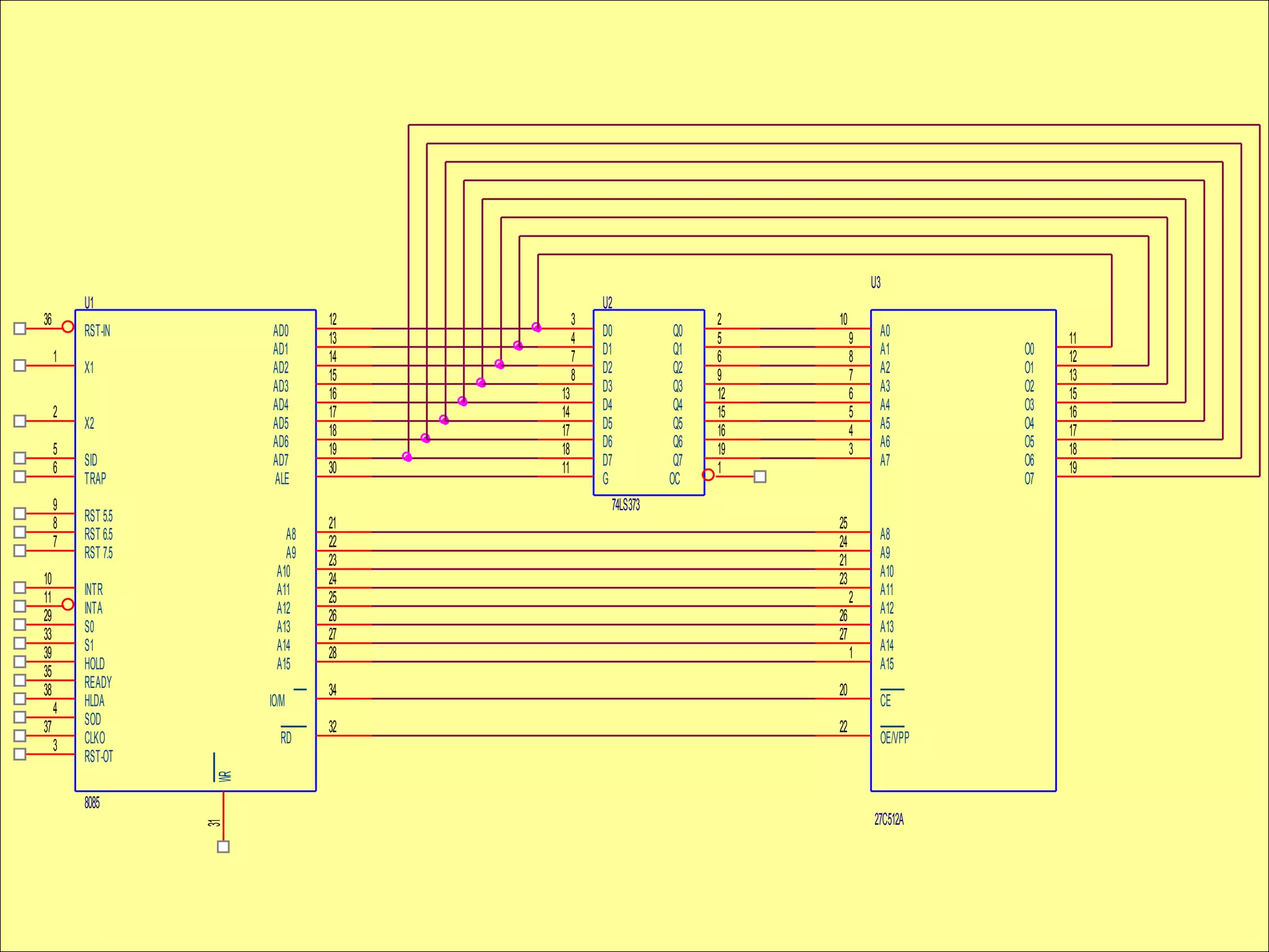
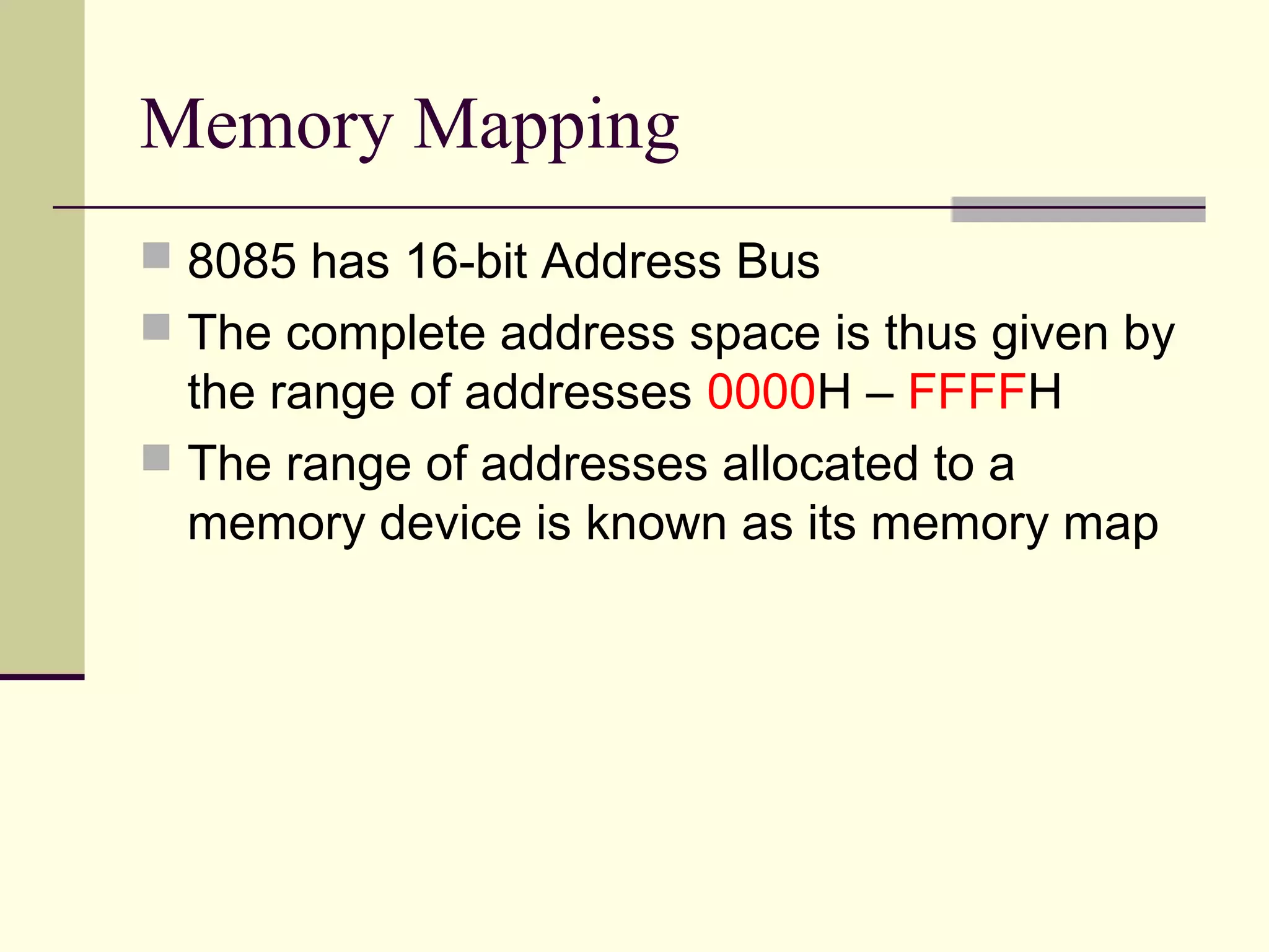
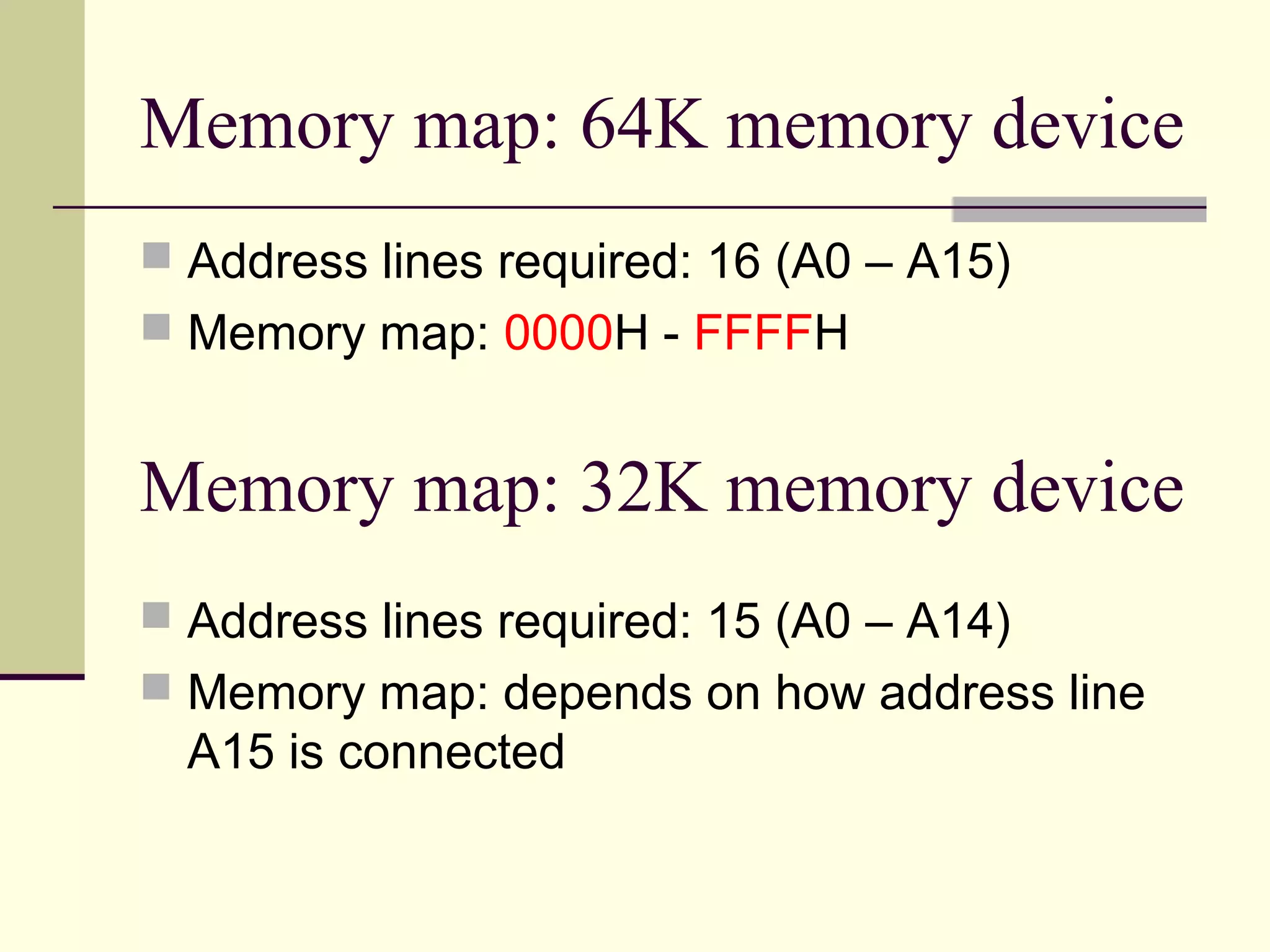
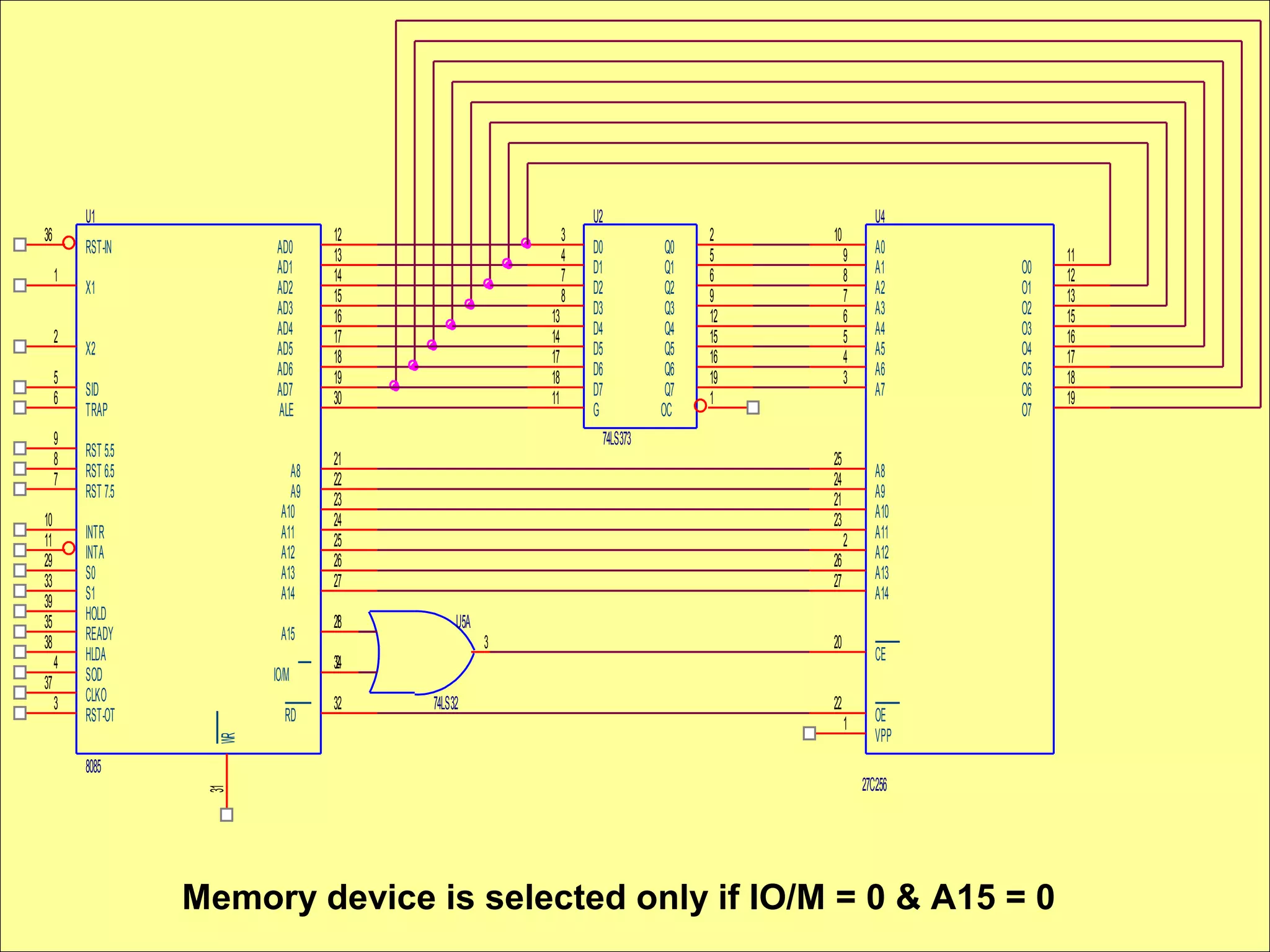
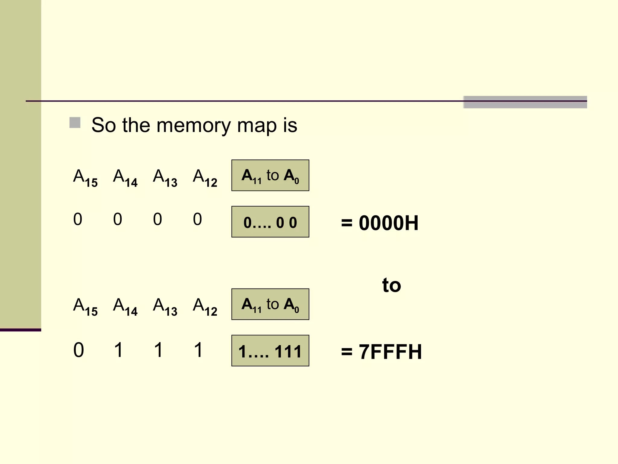
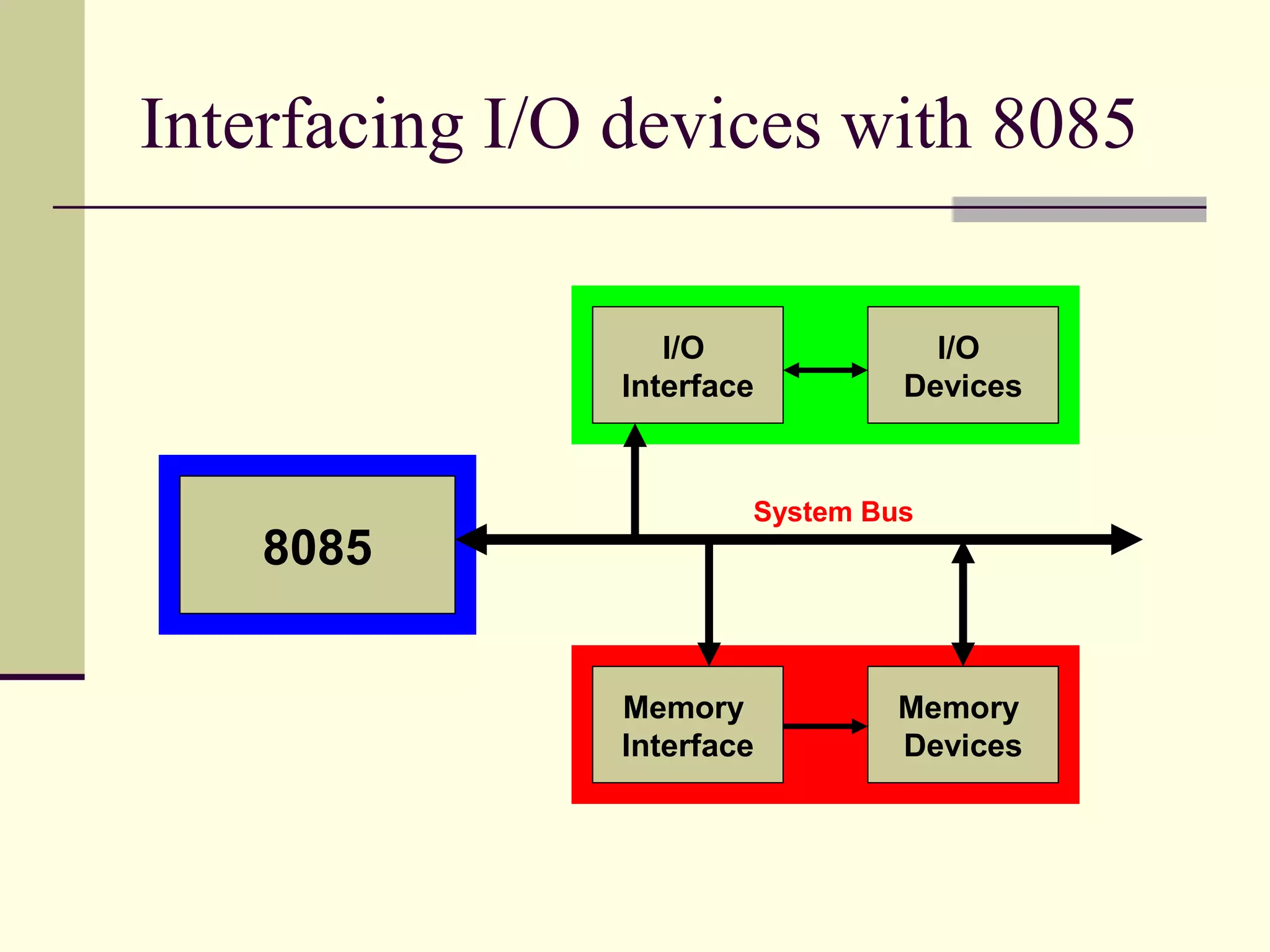
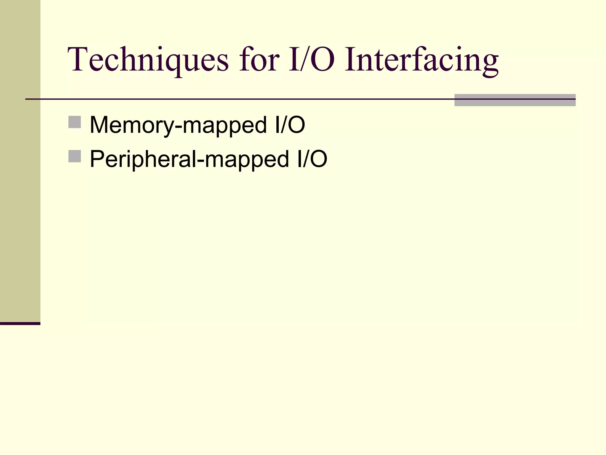
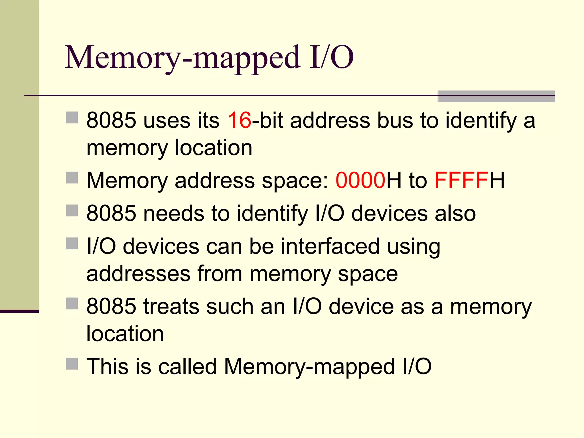
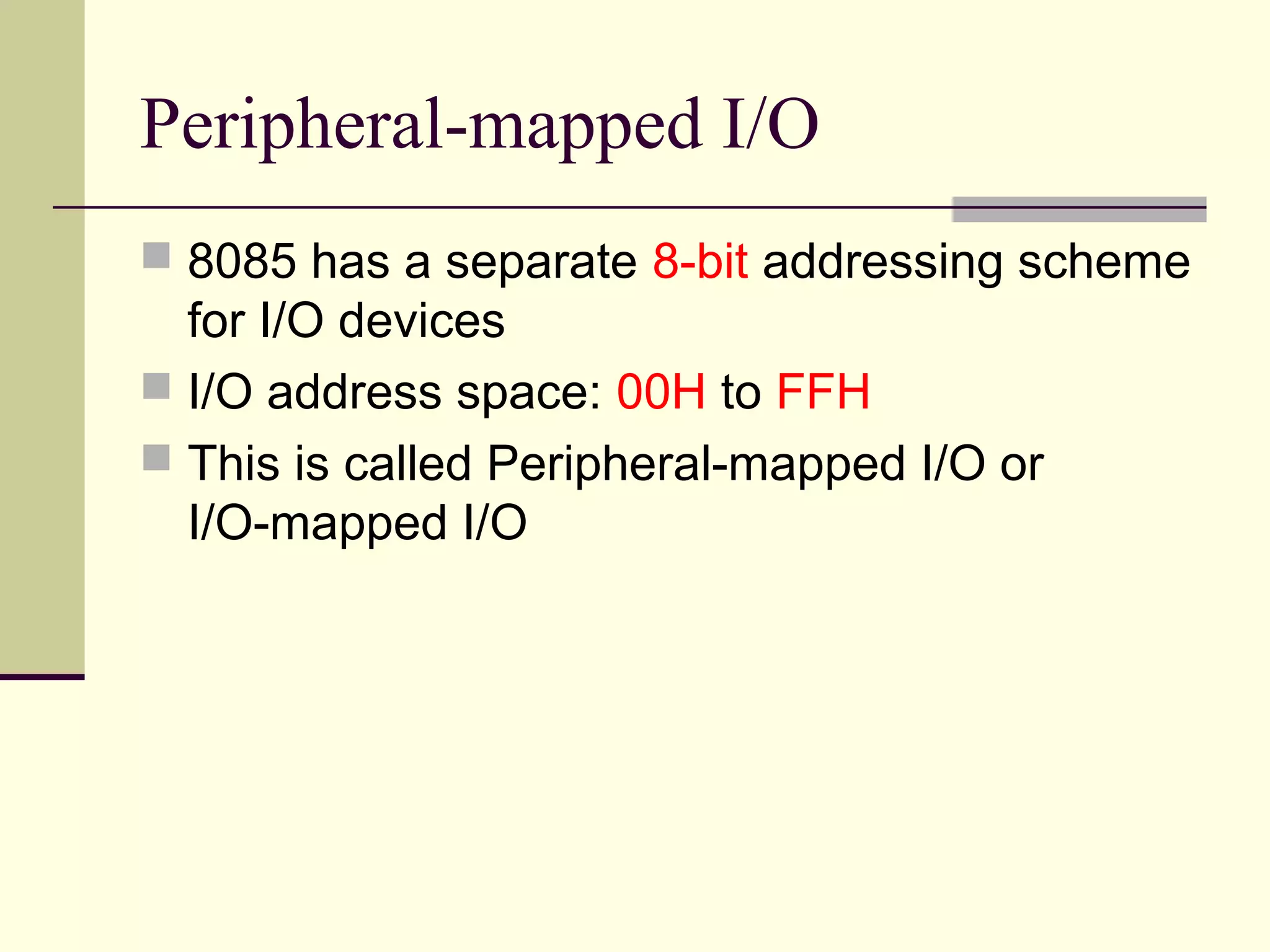
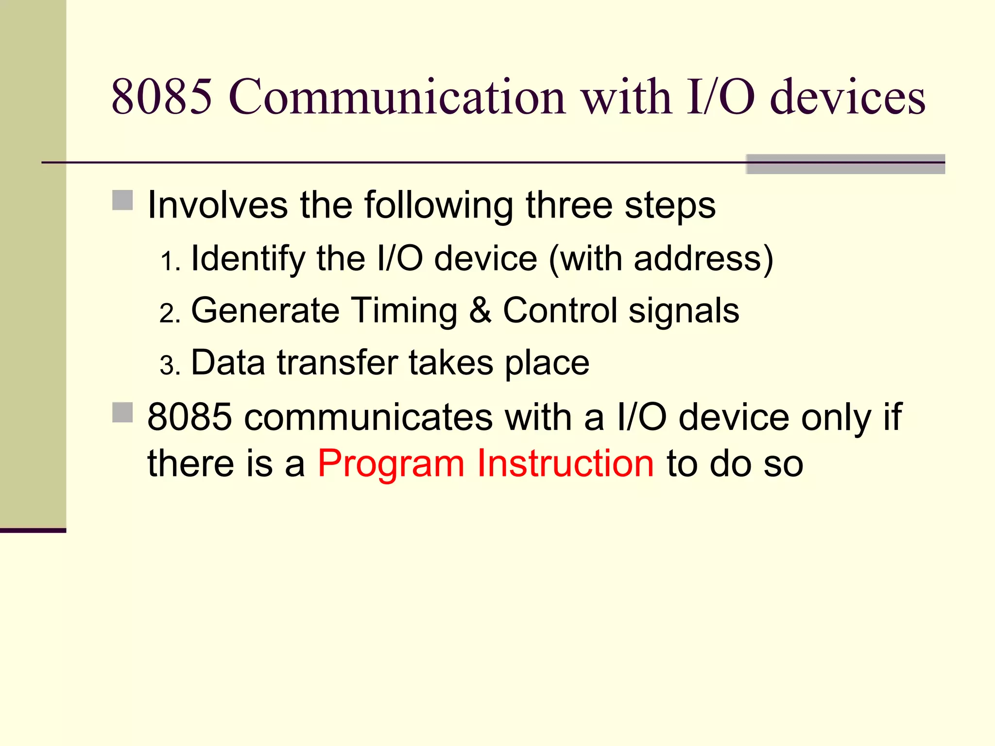
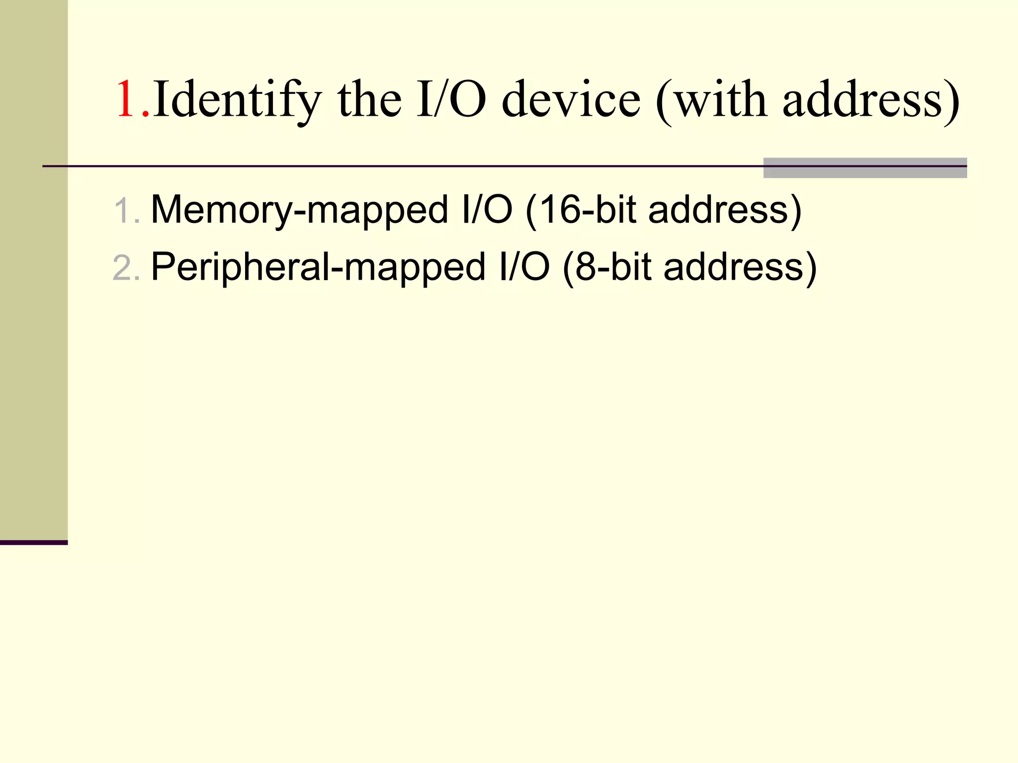
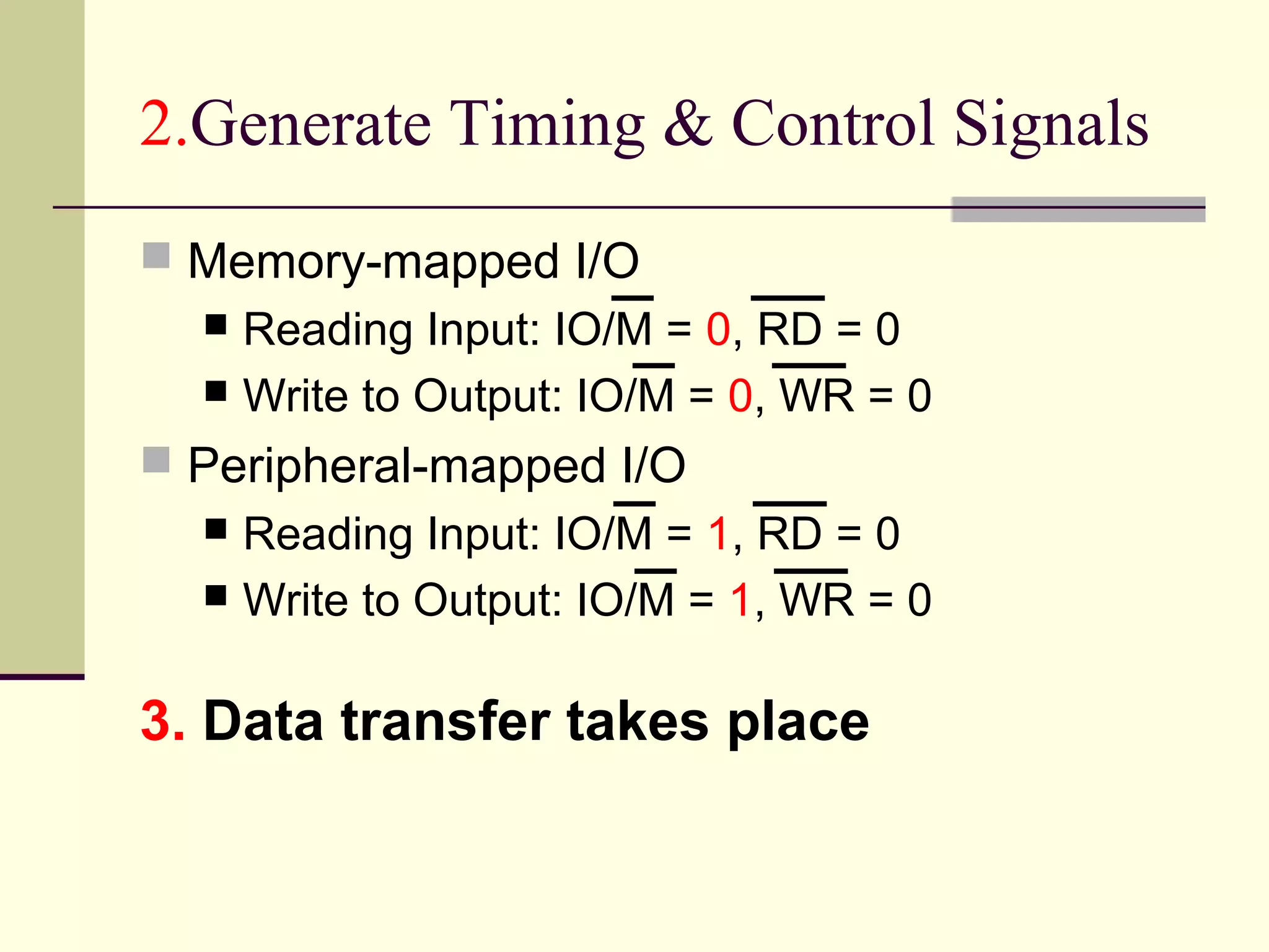
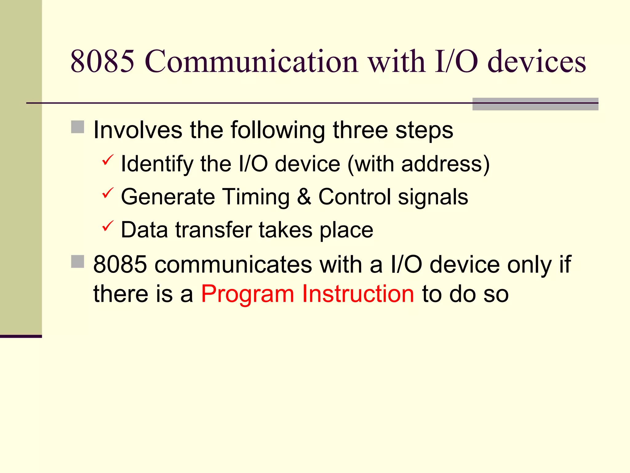
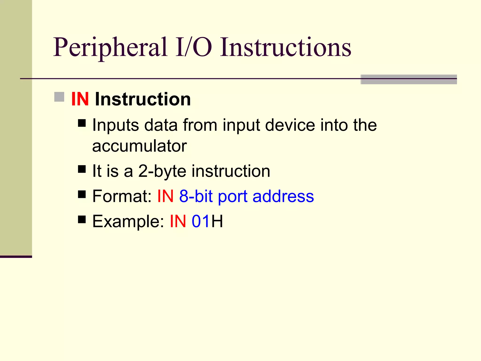
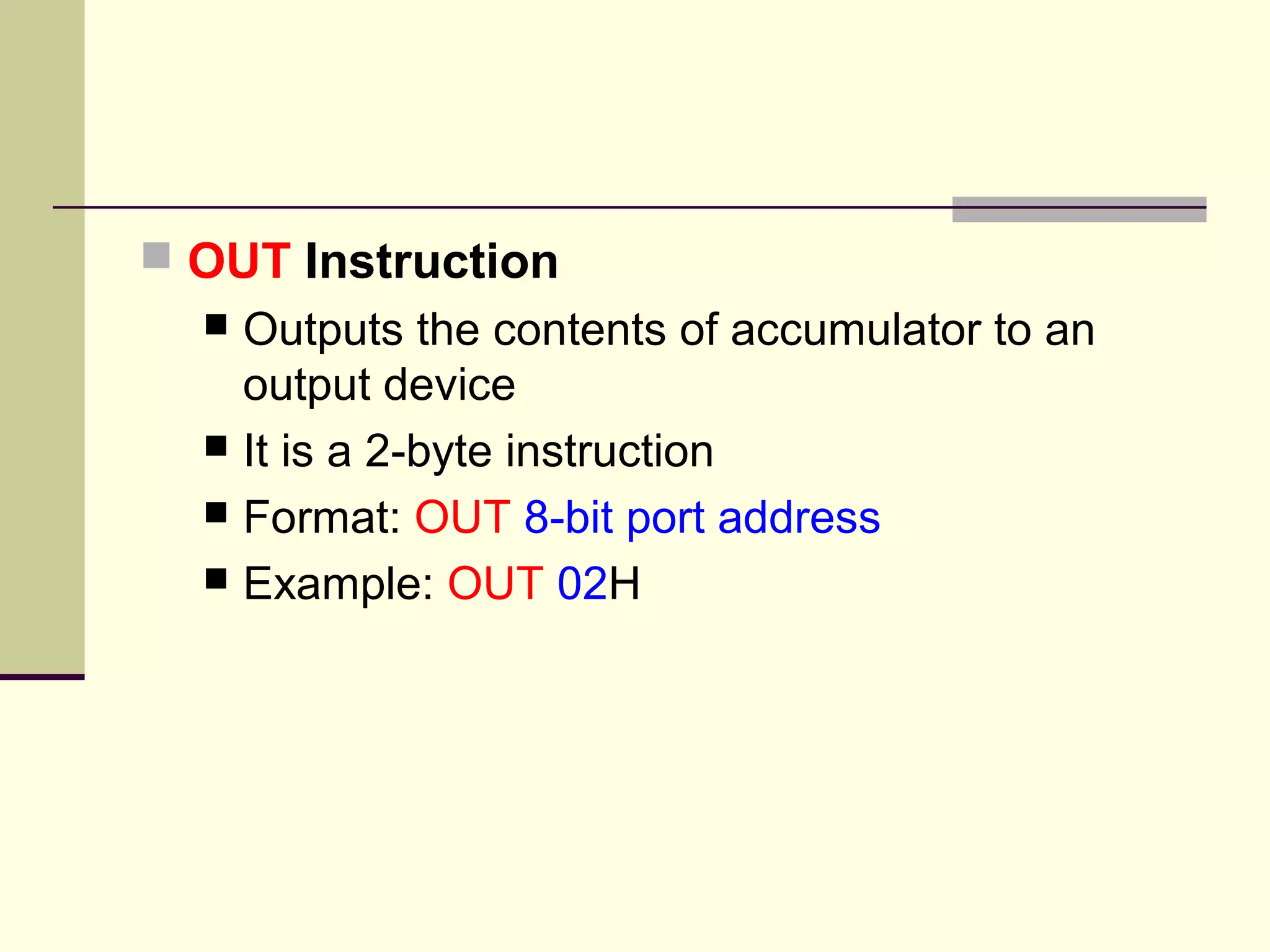
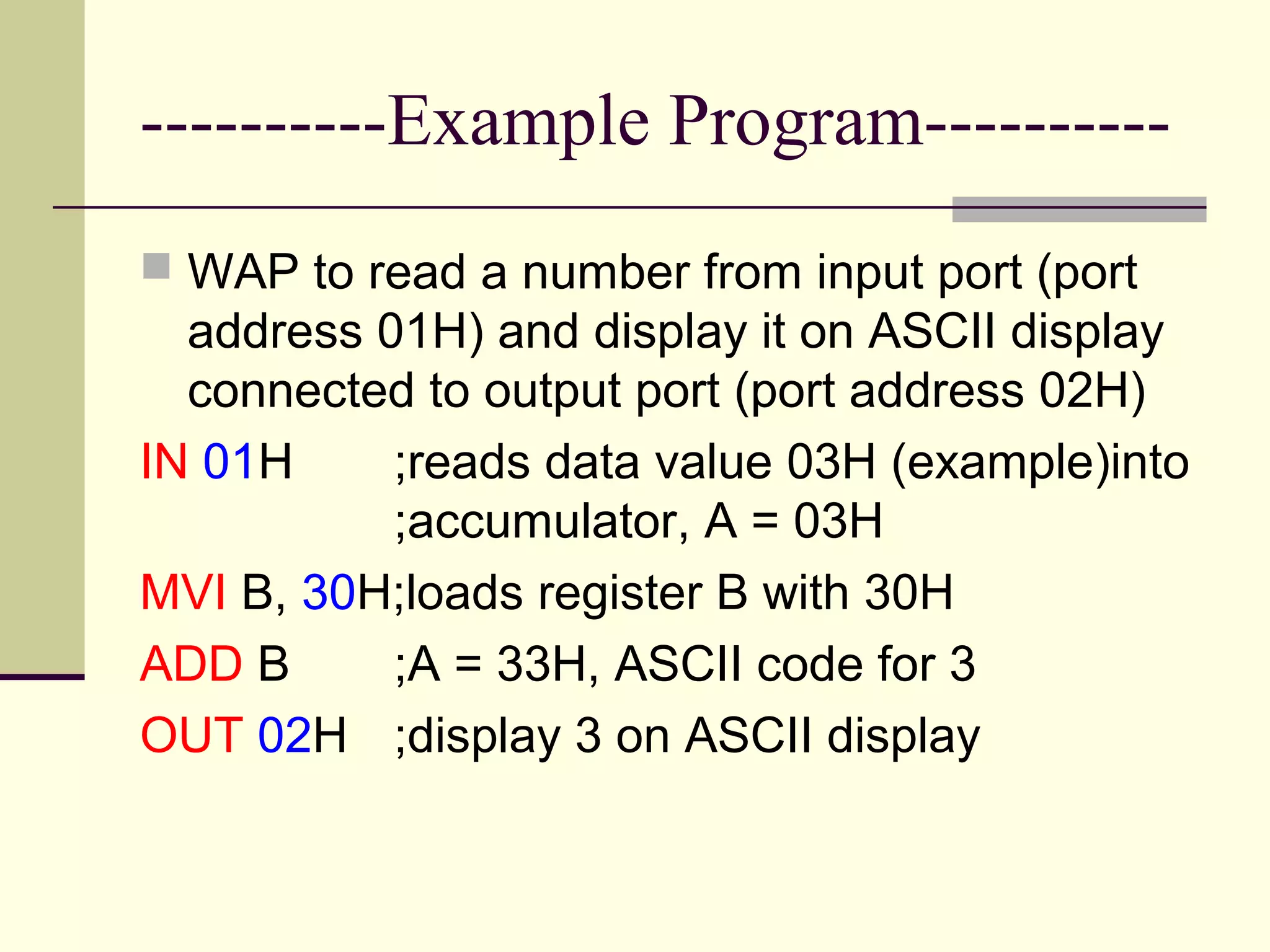
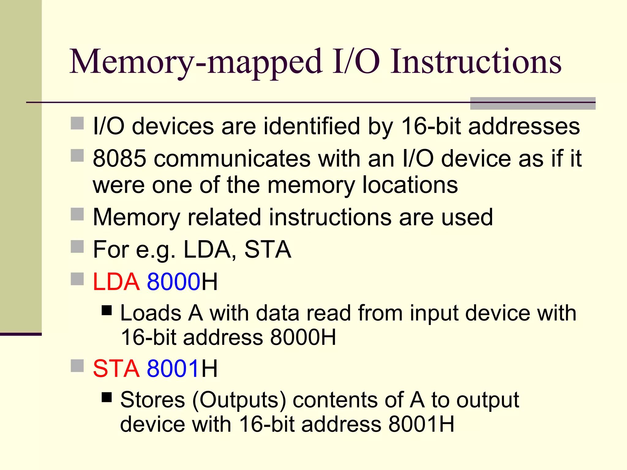
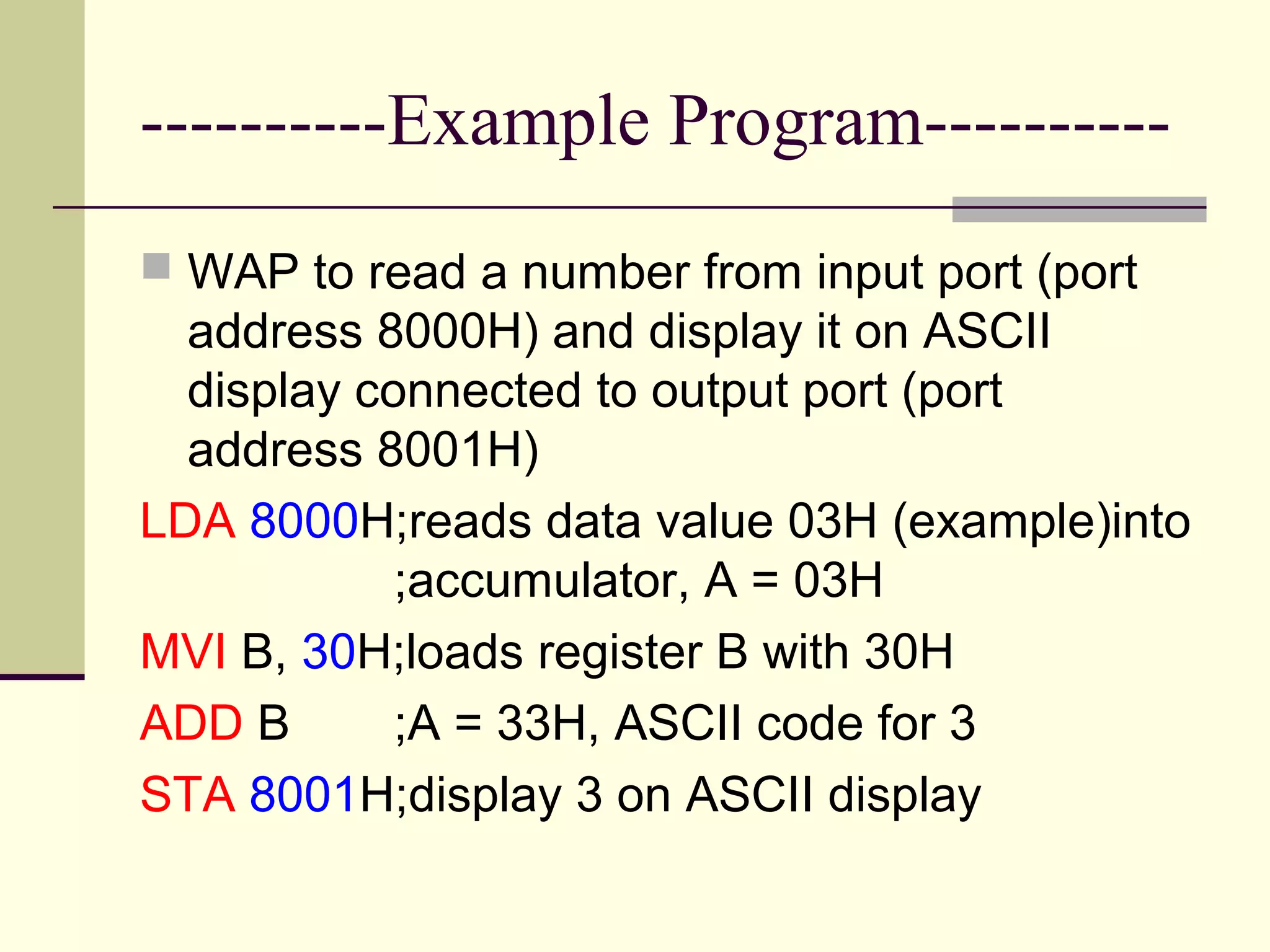
Md Zahidul Islam
lecturer at MIU
Welcome to all of you
8085 Microprocessor:
Architecture & Support Components
3
Microprocessor Architecture
 The microprocessor can be programmed to
perform functions on given data by writing
specific instructions into its memory.
 The microprocessor reads one instruction at a
time, matches it with its instruction set, and
performs the data manipulation specified.
 The result is either stored back into memory or
displayed on an output device.
Pinout Diagram of 8085
 A 40-pin IC
 Six groups of signals
 Address Bus
 Data Bus
 Control and Status pins
 Power Supply &
frequency signals
 Externally initiated
Signals
 Serial I/O ports
U7
8085
36
1
2
5
6
9
8
7
10
11
29
33
39
35
12
13
14
15
16
17
18
19
21
22
23
24
25
26
27
28
30
31
32
34
3
374
38
40
20
RST-IN
X1
X2
SID
TRAP
RST 5.5
RST 6.5
RST 7.5
INTR
INTA
S0
S1
HOLD
READY
AD0
AD1
AD2
AD3
AD4
AD5
AD6
AD7
A8
A9
A10
A11
A12
A13
A14
A15
ALE
WR
RD
IO/M
RST-OT
CLKOSOD
HLDA
VCC
VSS
Logic Pinout of 8085
DataBus
AddressBus
U8
8085
36
1
2
5
6
9
8
7
10
11
29
33
39
35
12
13
14
15
16
17
18
19
21
22
23
24
25
26
27
28
30
31
32
34
3
37
4
38
40
20
RST-IN
X1
X2
SID
TRAP
RST 5.5
RST 6.5
RST 7.5
INTR
INTA
S0
S1
HOLD
READY
AD0
AD1
AD2
AD3
AD4
AD5
AD6
AD7
A8
A9
A10
A11
A12
A13
A14
A15
ALE
WR
RD
IO/M
RST-OT
CLKO
SOD
HLDA
VCC
VSS
Control &
Status
Control &
Status
Externally
initiated
signals
Serial I/O
ports
Power Supply
& frequency
7
The 8085 Architecture
 The 8085 uses three separate busses to
perform its operations
 The address bus.
 The data bus.
 The control bus.
8
The Address Bus
 16 bits wide (A0 A1…A15)
 Therefore, the 8085 can access locations with
numbers from 0 to 65,536. Or, the 8085 can
access a total of 64K addresses.
 “Unidirectional”.
 Information flows out of the microprocessor and
into the memory or peripherals.
 When the 8085 wants to access a peripheral
or a memory location, it places the 16-bit
address on the address bus and then sends
9
The Data Bus
 8 bits wide (D0 D1…D7)
 “Bi-directional”.
 Information flows both ways between the
microprocessor and memory or I/O.
 The 8085 uses the data bus to transfer the
binary information.
 Since the data bus has 8-bits only, then the
8085 can manipulate data 8 bits at-a-time
only.
10
The Control Bus
 There is no real control bus. Instead, the
control bus is made up of a number of single
bit control signals.
8085 Operations
 Microprocessor Initiated Operations
 Internal Operations
 Peripheral/Externally Initiated Operations
Microprocessor Initiated Operations
 Memory Read
 Memory Write
 I/O Read
 I/O Write
13
Microprocessor Initiated
Operations
 These are operations that the microprocessor
itself starts.
 These are usually one of 4 operations:
 Memory Read
 Memory Write
 I/O Read (Get data from an input device)
 I/O write (Send data to an output device)
 Interrupt signal
14
Microprocessor Initiated Operations
 It is important to note that the microprocessor
treats memory and I/O devices the same way.
 The communication process between the
microprocessor and peripheral devices consist
of the following three steps:
 Identify the address.
 Transfer the binary information.
 Provide the right timing signals.
15
The Read Operation
 To read the contents of a memory location, the
following steps take place:
 The microprocessor places the 16-bit address of
the memory location on the address bus.
 The microprocessor activates a control signal
called “memory read” which enables the memory
chip.
 The memory decodes the address and identifies
the right location.
 The memory places the contents on the data bus.
 The microprocessor reads the value of the data
bus after a certain amount of time.
16
Internal Data Operations
 The 8085 can perform a number of internal
operations. Such as: storing data, Arithmetic
& Logic operations, Testing for condition, etc.
 To perform these operations, the
microprocessor needs an internal architecture
similar to the following:
Accumulator Flags
B C
D E
H L
Program Counter
Stack Pointer
DataAddress 816
Internal Operations
 Store 8-bit data
 Perform Arithmetic and Logic Operations
 Test for conditions
 Sequence the execution of instructions
 Store/Retrieve data from stack during
execution
18
The Internal Architecture
 We have already discussed the general
purpose registers, the Accumulator, and the
flags.
 The Program Counter (PC)
 This is a register that is used to control the
sequencing of the execution of instructions.
 This register always holds the address of the
next instruction.
 Since it holds an address, it must be 16 bits
wide.
19
The Internal Architecture
 The Stack pointer
 The stack pointer is also a 16-bit register that
is used to point into memory.
 The memory this register points to is a special
area called the stack.
 The stack is an area of memory used to hold
data that will be retreived soon.
 The stack is usually accessed in a Last In First
Out (LIFO) fashion.
Peripheral/Externally Initiated
Operations
 Reset
 Interrupt
 Ready
 Hold
21
Externally Initiated Operations
 External devices can initiate (start) one of the
4 following operations:
 Reset
 All operations are stopped and the program
counter is reset to 0000.
 Interrupt
 The microprocessor’s operations are interrupted
and the microprocessor executes what is called a
“service routine”.
 This routine “handles” the interrupt, (perform the
necessary operations). Then the microprocessor
returns to its previous operations and continues.
22
Externally Initiated Operations
 Ready
 The 8085 has a pin called RDY. This pin is used
by external devices to stop the 8085 until they
catch up.
 As long as the RDY pin is low, the 8085 will be in
a wait state.
 Hold
 The 8085 has a pin called HOLD. This pin is
used by external devices to gain control of the
busses.
 When the HOLD signal is activated by an
external device, the 8085 stops executing
instructions and stops using the busses.
Architecture of 8085
 Power Supply – a +5V DC power supply
 Maximum clock frequency of 3MHz
 8-bit general purpose microprocessor
 16-bit Address Bus
 Capable of addressing 64K of memory
Architecture of 8085
Architecture 0f 8085 Cont…
 ALU
 Timing and Control Unit
 General Purpose
Registers
 Program Status word
 Program Counter
 Stack Pointer
 Instruction Register and
Decoder
 Interrupt Control
 Serial I/O Control
 Address Bus
 Data Bus
Architecture 0f 8085 Cont…
 Arithmetic Logic Unit (ALU)
 8085 has 8-bit ALU
 Performs arithmetic & Logic operations on
data
 Timing & Control Unit
 Generates timing and control signals
 General Purpose Registers
 8-bit registers (B,C,D,E,H,L)
 16-bit register pairs (BC, DE, HL,PSW)
Architecture 0f 8085 Cont…
 Program Status Word (PSW)
 Accumulator and Flag Register can be
combined as a register pair called PSW
 Instruction Register and Decoder
 Instruction fetched from memory is stored in
Instruction register (8-bit register)
 Decoder decodes the instruction and directs
the Timing & Control Unit accordingly
Architecture 0f 8085 Cont…
 Interrupt Control
 8085 has 5 interrupt signals
 INTR – general purpose interrupt
 RST 5.5 Restart Interrupts
 RST 6.5
 RST 7.5
 TRAP – non-maskable interrupt
 The interrupts listed above are in increasing
order of priority
Architecture 0f 8085 Cont…
 Serial I/O Control
 8085 has two signals for serial communication
 SID – Serial Input Data
 SOD – Serial Output Data
Architecture 0f 8085 Cont…
 Address Bus
 Used to address memory & I/O devices
 8085 has a 16-bit address bus
A15 A14 A13 A12 A11 A10 A9 A8
AD7 AD6 AD5 AD4 AD3 AD2 AD1 AD0
Lower-order AddressHigher-order Address
 Data Bus
 Used to transfer instructions and data
 8085 has a 8-bit data bus
Data Bus
8085 Communication with Memory
 Involves the following three steps
1. Identify the memory location (with address)
2. Generate Timing & Control signals
3. Data transfer takes place
Example: Memory Read Operation
1
2
3
1
2
3
Timing Diagram
Demultiplexing Address/Data Bus
 8085 identifies a memory location with its 16
address lines, (AD0 to AD7) & (A8 to A15)
 8085 performs data transfer using its data
lines, AD0 to AD7
 Lower order address bus & Data bus are
multiplexed on same lines i.e. AD0 to AD7.
 Demultiplexing refers to separating Address &
Data signals for read/write operations
Need for Demultiplexing…
8085 Memory
A8-A15
20H
AD0-AD7
05H
RD
4FH 2005H
 The 16-bit address of the memory location
must be applied to the memory chip for the
whole duration of the memory read/write
operation.
 Lower-order address needs to be saved
before microprocessor uses it for data
transfer
Need for Demultiplexing…
8085 Interfacing with Memory chips
8085
Memory
Interface
Memory
Chip
Address
Data
Control
Address
Data
Control
8085 Interfacing with Memory chips
8085
Memory
Interface
Memory
Chip
AD0-AD7
Control
A0 – A7
Data
74LS373
A8-A15 A8-A15
ALE
8085 Interfacing with Memory chips
8085
Memory
Interface
Program
Memory
AD0-AD7
IO/M
A0 – A7
Data
74LS373
A8-A15 A8-A15
ALE
RD
RD
CS
U2
74LS373
3
4
7
8
13
14
17
18
111
2
5
6
9
12
15
16
19
D0
D1
D2
D3
D4
D5
D6
D7
OCG
Q0
Q1
Q2
Q3
Q4
Q5
Q6
Q7
U1
8085
36
1
2
5
6
9
8
7
10
11
29
33
39
35
12
13
14
15
16
17
18
19
21
22
23
24
25
26
27
28
30
31
32
34
3
37
4
38
RST-IN
X1
X2
SID
TRAP
RST 5.5
RST 6.5
RST 7.5
INTR
INTA
S0
S1
HOLD
READY
AD0
AD1
AD2
AD3
AD4
AD5
AD6
AD7
A8
A9
A10
A11
A12
A13
A14
A15
ALE
WR
RD
IO/M
RST-OT
CLKO
SOD
HLDA
U3
27C512A
10
9
8
7
6
5
4
3
25
24
21
23
2
26
20
22
27
1
11
12
13
15
16
17
18
19
A0
A1
A2
A3
A4
A5
A6
A7
A8
A9
A10
A11
A12
A13
CE
OE/VPP
A14
A15
O0
O1
O2
O3
O4
O5
O6
O7
Memory Mapping
 8085 has 16-bit Address Bus
 The complete address space is thus given by
the range of addresses 0000H – FFFFH
 The range of addresses allocated to a
memory device is known as its memory map
Memory map: 64K memory device
 Address lines required: 16 (A0 – A15)
 Memory map: 0000H - FFFFH
Memory map: 32K memory device
 Address lines required: 15 (A0 – A14)
 Memory map: depends on how address line
A15 is connected
U1
8085
36
1
2
5
6
9
8
7
10
11
29
33
39
35
12
13
14
15
16
17
18
19
21
22
23
24
25
26
27
28
30
31
32
34
3
37
4
38
RST-IN
X1
X2
SID
TRAP
RST 5.5
RST 6.5
RST 7.5
INTR
INTA
S0
S1
HOLD
READY
AD0
AD1
AD2
AD3
AD4
AD5
AD6
AD7
A8
A9
A10
A11
A12
A13
A14
A15
ALE
WR
RD
IO/M
RST-OT
CLKO
SOD
HLDA
U2
74LS373
3
4
7
8
13
14
17
18
111
2
5
6
9
12
15
16
19
D0
D1
D2
D3
D4
D5
D6
D7
OCG
Q0
Q1
Q2
Q3
Q4
Q5
Q6
Q7
U4
27C256
10
9
8
7
6
5
4
3
25
24
21
23
2
26
27
20
22
1
11
12
13
15
16
17
18
19
A0
A1
A2
A3
A4
A5
A6
A7
A8
A9
A10
A11
A12
A13
A14
CE
OE
VPP
O0
O1
O2
O3
O4
O5
O6
O7
U5A
74LS32
1
2
3
Memory device is selected only if IO/M = 0 & A15 = 0
 So the memory map is
0 0 0 0
A11 to A0A15 A14 A13 A12
0…. 0 0 = 0000H
0 1 1 1
A11 to A0A15 A14 A13 A12
1…. 111 = 7FFFH
to
Interfacing I/O devices
with 8085
Peripheral-mapped I/O
&
Memory-mapped I/O
Interfacing I/O devices with 8085
8085
I/O
Interface
I/O
Devices
Memory
Interface
Memory
Devices
System Bus
Techniques for I/O Interfacing
 Memory-mapped I/O
 Peripheral-mapped I/O
Memory-mapped I/O
 8085 uses its 16-bit address bus to identify a
memory location
 Memory address space: 0000H to FFFFH
 8085 needs to identify I/O devices also
 I/O devices can be interfaced using
addresses from memory space
 8085 treats such an I/O device as a memory
location
 This is called Memory-mapped I/O
Peripheral-mapped I/O
 8085 has a separate 8-bit addressing scheme
for I/O devices
 I/O address space: 00H to FFH
 This is called Peripheral-mapped I/O or
I/O-mapped I/O
8085 Communication with I/O devices
 Involves the following three steps
1. Identify the I/O device (with address)
2. Generate Timing & Control signals
3. Data transfer takes place
 8085 communicates with a I/O device only if
there is a Program Instruction to do so
1.Identify the I/O device (with address)
1. Memory-mapped I/O (16-bit address)
2. Peripheral-mapped I/O (8-bit address)
2.Generate Timing & Control Signals
 Memory-mapped I/O
 Reading Input: IO/M = 0, RD = 0
 Write to Output: IO/M = 0, WR = 0
 Peripheral-mapped I/O
 Reading Input: IO/M = 1, RD = 0
 Write to Output: IO/M = 1, WR = 0
3. Data transfer takes place
8085 Communication with I/O devices
 Involves the following three steps
 Identify the I/O device (with address)
 Generate Timing & Control signals
 Data transfer takes place
 8085 communicates with a I/O device only if
there is a Program Instruction to do so
Peripheral I/O Instructions
 IN Instruction
 Inputs data from input device into the
accumulator
 It is a 2-byte instruction
 Format: IN 8-bit port address
 Example: IN 01H
 OUT Instruction
 Outputs the contents of accumulator to an
output device
 It is a 2-byte instruction
 Format: OUT 8-bit port address
 Example: OUT 02H
----------Example Program----------
 WAP to read a number from input port (port
address 01H) and display it on ASCII display
connected to output port (port address 02H)
IN 01H ;reads data value 03H (example)into
;accumulator, A = 03H
MVI B, 30H;loads register B with 30H
ADD B ;A = 33H, ASCII code for 3
OUT 02H ;display 3 on ASCII display
Memory-mapped I/O Instructions
 I/O devices are identified by 16-bit addresses
 8085 communicates with an I/O device as if it
were one of the memory locations
 Memory related instructions are used
 For e.g. LDA, STA
 LDA 8000H
 Loads A with data read from input device with
16-bit address 8000H
 STA 8001H
 Stores (Outputs) contents of A to output
device with 16-bit address 8001H
----------Example Program----------
 WAP to read a number from input port (port
address 8000H) and display it on ASCII
display connected to output port (port
address 8001H)
LDA 8000H;reads data value 03H (example)into
;accumulator, A = 03H
MVI B, 30H;loads register B with 30H
ADD B ;A = 33H, ASCII code for 3
STA 8001H;display 3 on ASCII display

architecture memory interfacing

  • 1.
    Md Zahidul Islam lecturerat MIU Welcome to all of you
  • 2.
  • 3.
    3 Microprocessor Architecture  Themicroprocessor can be programmed to perform functions on given data by writing specific instructions into its memory.  The microprocessor reads one instruction at a time, matches it with its instruction set, and performs the data manipulation specified.  The result is either stored back into memory or displayed on an output device.
  • 5.
    Pinout Diagram of8085  A 40-pin IC  Six groups of signals  Address Bus  Data Bus  Control and Status pins  Power Supply & frequency signals  Externally initiated Signals  Serial I/O ports U7 8085 36 1 2 5 6 9 8 7 10 11 29 33 39 35 12 13 14 15 16 17 18 19 21 22 23 24 25 26 27 28 30 31 32 34 3 374 38 40 20 RST-IN X1 X2 SID TRAP RST 5.5 RST 6.5 RST 7.5 INTR INTA S0 S1 HOLD READY AD0 AD1 AD2 AD3 AD4 AD5 AD6 AD7 A8 A9 A10 A11 A12 A13 A14 A15 ALE WR RD IO/M RST-OT CLKOSOD HLDA VCC VSS
  • 6.
    Logic Pinout of8085 DataBus AddressBus U8 8085 36 1 2 5 6 9 8 7 10 11 29 33 39 35 12 13 14 15 16 17 18 19 21 22 23 24 25 26 27 28 30 31 32 34 3 37 4 38 40 20 RST-IN X1 X2 SID TRAP RST 5.5 RST 6.5 RST 7.5 INTR INTA S0 S1 HOLD READY AD0 AD1 AD2 AD3 AD4 AD5 AD6 AD7 A8 A9 A10 A11 A12 A13 A14 A15 ALE WR RD IO/M RST-OT CLKO SOD HLDA VCC VSS Control & Status Control & Status Externally initiated signals Serial I/O ports Power Supply & frequency
  • 7.
    7 The 8085 Architecture The 8085 uses three separate busses to perform its operations  The address bus.  The data bus.  The control bus.
  • 8.
    8 The Address Bus 16 bits wide (A0 A1…A15)  Therefore, the 8085 can access locations with numbers from 0 to 65,536. Or, the 8085 can access a total of 64K addresses.  “Unidirectional”.  Information flows out of the microprocessor and into the memory or peripherals.  When the 8085 wants to access a peripheral or a memory location, it places the 16-bit address on the address bus and then sends
  • 9.
    9 The Data Bus 8 bits wide (D0 D1…D7)  “Bi-directional”.  Information flows both ways between the microprocessor and memory or I/O.  The 8085 uses the data bus to transfer the binary information.  Since the data bus has 8-bits only, then the 8085 can manipulate data 8 bits at-a-time only.
  • 10.
    10 The Control Bus There is no real control bus. Instead, the control bus is made up of a number of single bit control signals.
  • 11.
    8085 Operations  MicroprocessorInitiated Operations  Internal Operations  Peripheral/Externally Initiated Operations
  • 12.
    Microprocessor Initiated Operations Memory Read  Memory Write  I/O Read  I/O Write
  • 13.
    13 Microprocessor Initiated Operations  Theseare operations that the microprocessor itself starts.  These are usually one of 4 operations:  Memory Read  Memory Write  I/O Read (Get data from an input device)  I/O write (Send data to an output device)  Interrupt signal
  • 14.
    14 Microprocessor Initiated Operations It is important to note that the microprocessor treats memory and I/O devices the same way.  The communication process between the microprocessor and peripheral devices consist of the following three steps:  Identify the address.  Transfer the binary information.  Provide the right timing signals.
  • 15.
    15 The Read Operation To read the contents of a memory location, the following steps take place:  The microprocessor places the 16-bit address of the memory location on the address bus.  The microprocessor activates a control signal called “memory read” which enables the memory chip.  The memory decodes the address and identifies the right location.  The memory places the contents on the data bus.  The microprocessor reads the value of the data bus after a certain amount of time.
  • 16.
    16 Internal Data Operations The 8085 can perform a number of internal operations. Such as: storing data, Arithmetic & Logic operations, Testing for condition, etc.  To perform these operations, the microprocessor needs an internal architecture similar to the following: Accumulator Flags B C D E H L Program Counter Stack Pointer DataAddress 816
  • 17.
    Internal Operations  Store8-bit data  Perform Arithmetic and Logic Operations  Test for conditions  Sequence the execution of instructions  Store/Retrieve data from stack during execution
  • 18.
    18 The Internal Architecture We have already discussed the general purpose registers, the Accumulator, and the flags.  The Program Counter (PC)  This is a register that is used to control the sequencing of the execution of instructions.  This register always holds the address of the next instruction.  Since it holds an address, it must be 16 bits wide.
  • 19.
    19 The Internal Architecture The Stack pointer  The stack pointer is also a 16-bit register that is used to point into memory.  The memory this register points to is a special area called the stack.  The stack is an area of memory used to hold data that will be retreived soon.  The stack is usually accessed in a Last In First Out (LIFO) fashion.
  • 20.
  • 21.
    21 Externally Initiated Operations External devices can initiate (start) one of the 4 following operations:  Reset  All operations are stopped and the program counter is reset to 0000.  Interrupt  The microprocessor’s operations are interrupted and the microprocessor executes what is called a “service routine”.  This routine “handles” the interrupt, (perform the necessary operations). Then the microprocessor returns to its previous operations and continues.
  • 22.
    22 Externally Initiated Operations Ready  The 8085 has a pin called RDY. This pin is used by external devices to stop the 8085 until they catch up.  As long as the RDY pin is low, the 8085 will be in a wait state.  Hold  The 8085 has a pin called HOLD. This pin is used by external devices to gain control of the busses.  When the HOLD signal is activated by an external device, the 8085 stops executing instructions and stops using the busses.
  • 23.
    Architecture of 8085 Power Supply – a +5V DC power supply  Maximum clock frequency of 3MHz  8-bit general purpose microprocessor  16-bit Address Bus  Capable of addressing 64K of memory
  • 24.
  • 25.
    Architecture 0f 8085Cont…  ALU  Timing and Control Unit  General Purpose Registers  Program Status word  Program Counter  Stack Pointer  Instruction Register and Decoder  Interrupt Control  Serial I/O Control  Address Bus  Data Bus
  • 26.
    Architecture 0f 8085Cont…  Arithmetic Logic Unit (ALU)  8085 has 8-bit ALU  Performs arithmetic & Logic operations on data  Timing & Control Unit  Generates timing and control signals  General Purpose Registers  8-bit registers (B,C,D,E,H,L)  16-bit register pairs (BC, DE, HL,PSW)
  • 27.
    Architecture 0f 8085Cont…  Program Status Word (PSW)  Accumulator and Flag Register can be combined as a register pair called PSW  Instruction Register and Decoder  Instruction fetched from memory is stored in Instruction register (8-bit register)  Decoder decodes the instruction and directs the Timing & Control Unit accordingly
  • 28.
    Architecture 0f 8085Cont…  Interrupt Control  8085 has 5 interrupt signals  INTR – general purpose interrupt  RST 5.5 Restart Interrupts  RST 6.5  RST 7.5  TRAP – non-maskable interrupt  The interrupts listed above are in increasing order of priority
  • 29.
    Architecture 0f 8085Cont…  Serial I/O Control  8085 has two signals for serial communication  SID – Serial Input Data  SOD – Serial Output Data
  • 30.
  • 31.
    Architecture 0f 8085Cont…  Address Bus  Used to address memory & I/O devices  8085 has a 16-bit address bus A15 A14 A13 A12 A11 A10 A9 A8 AD7 AD6 AD5 AD4 AD3 AD2 AD1 AD0 Lower-order AddressHigher-order Address  Data Bus  Used to transfer instructions and data  8085 has a 8-bit data bus Data Bus
  • 32.
    8085 Communication withMemory  Involves the following three steps 1. Identify the memory location (with address) 2. Generate Timing & Control signals 3. Data transfer takes place
  • 33.
    Example: Memory ReadOperation 1 2 3
  • 34.
  • 35.
  • 36.
    Demultiplexing Address/Data Bus 8085 identifies a memory location with its 16 address lines, (AD0 to AD7) & (A8 to A15)  8085 performs data transfer using its data lines, AD0 to AD7  Lower order address bus & Data bus are multiplexed on same lines i.e. AD0 to AD7.  Demultiplexing refers to separating Address & Data signals for read/write operations
  • 37.
    Need for Demultiplexing… 8085Memory A8-A15 20H AD0-AD7 05H RD 4FH 2005H
  • 38.
     The 16-bitaddress of the memory location must be applied to the memory chip for the whole duration of the memory read/write operation.  Lower-order address needs to be saved before microprocessor uses it for data transfer Need for Demultiplexing…
  • 40.
    8085 Interfacing withMemory chips 8085 Memory Interface Memory Chip Address Data Control Address Data Control
  • 41.
    8085 Interfacing withMemory chips 8085 Memory Interface Memory Chip AD0-AD7 Control A0 – A7 Data 74LS373 A8-A15 A8-A15 ALE
  • 42.
    8085 Interfacing withMemory chips 8085 Memory Interface Program Memory AD0-AD7 IO/M A0 – A7 Data 74LS373 A8-A15 A8-A15 ALE RD RD CS
  • 43.
    U2 74LS373 3 4 7 8 13 14 17 18 111 2 5 6 9 12 15 16 19 D0 D1 D2 D3 D4 D5 D6 D7 OCG Q0 Q1 Q2 Q3 Q4 Q5 Q6 Q7 U1 8085 36 1 2 5 6 9 8 7 10 11 29 33 39 35 12 13 14 15 16 17 18 19 21 22 23 24 25 26 27 28 30 31 32 34 3 37 4 38 RST-IN X1 X2 SID TRAP RST 5.5 RST 6.5 RST7.5 INTR INTA S0 S1 HOLD READY AD0 AD1 AD2 AD3 AD4 AD5 AD6 AD7 A8 A9 A10 A11 A12 A13 A14 A15 ALE WR RD IO/M RST-OT CLKO SOD HLDA U3 27C512A 10 9 8 7 6 5 4 3 25 24 21 23 2 26 20 22 27 1 11 12 13 15 16 17 18 19 A0 A1 A2 A3 A4 A5 A6 A7 A8 A9 A10 A11 A12 A13 CE OE/VPP A14 A15 O0 O1 O2 O3 O4 O5 O6 O7
  • 44.
    Memory Mapping  8085has 16-bit Address Bus  The complete address space is thus given by the range of addresses 0000H – FFFFH  The range of addresses allocated to a memory device is known as its memory map
  • 45.
    Memory map: 64Kmemory device  Address lines required: 16 (A0 – A15)  Memory map: 0000H - FFFFH Memory map: 32K memory device  Address lines required: 15 (A0 – A14)  Memory map: depends on how address line A15 is connected
  • 46.
    U1 8085 36 1 2 5 6 9 8 7 10 11 29 33 39 35 12 13 14 15 16 17 18 19 21 22 23 24 25 26 27 28 30 31 32 34 3 37 4 38 RST-IN X1 X2 SID TRAP RST 5.5 RST 6.5 RST7.5 INTR INTA S0 S1 HOLD READY AD0 AD1 AD2 AD3 AD4 AD5 AD6 AD7 A8 A9 A10 A11 A12 A13 A14 A15 ALE WR RD IO/M RST-OT CLKO SOD HLDA U2 74LS373 3 4 7 8 13 14 17 18 111 2 5 6 9 12 15 16 19 D0 D1 D2 D3 D4 D5 D6 D7 OCG Q0 Q1 Q2 Q3 Q4 Q5 Q6 Q7 U4 27C256 10 9 8 7 6 5 4 3 25 24 21 23 2 26 27 20 22 1 11 12 13 15 16 17 18 19 A0 A1 A2 A3 A4 A5 A6 A7 A8 A9 A10 A11 A12 A13 A14 CE OE VPP O0 O1 O2 O3 O4 O5 O6 O7 U5A 74LS32 1 2 3 Memory device is selected only if IO/M = 0 & A15 = 0
  • 47.
     So thememory map is 0 0 0 0 A11 to A0A15 A14 A13 A12 0…. 0 0 = 0000H 0 1 1 1 A11 to A0A15 A14 A13 A12 1…. 111 = 7FFFH to
  • 48.
    Interfacing I/O devices with8085 Peripheral-mapped I/O & Memory-mapped I/O
  • 49.
    Interfacing I/O deviceswith 8085 8085 I/O Interface I/O Devices Memory Interface Memory Devices System Bus
  • 50.
    Techniques for I/OInterfacing  Memory-mapped I/O  Peripheral-mapped I/O
  • 51.
    Memory-mapped I/O  8085uses its 16-bit address bus to identify a memory location  Memory address space: 0000H to FFFFH  8085 needs to identify I/O devices also  I/O devices can be interfaced using addresses from memory space  8085 treats such an I/O device as a memory location  This is called Memory-mapped I/O
  • 52.
    Peripheral-mapped I/O  8085has a separate 8-bit addressing scheme for I/O devices  I/O address space: 00H to FFH  This is called Peripheral-mapped I/O or I/O-mapped I/O
  • 53.
    8085 Communication withI/O devices  Involves the following three steps 1. Identify the I/O device (with address) 2. Generate Timing & Control signals 3. Data transfer takes place  8085 communicates with a I/O device only if there is a Program Instruction to do so
  • 54.
    1.Identify the I/Odevice (with address) 1. Memory-mapped I/O (16-bit address) 2. Peripheral-mapped I/O (8-bit address)
  • 55.
    2.Generate Timing &Control Signals  Memory-mapped I/O  Reading Input: IO/M = 0, RD = 0  Write to Output: IO/M = 0, WR = 0  Peripheral-mapped I/O  Reading Input: IO/M = 1, RD = 0  Write to Output: IO/M = 1, WR = 0 3. Data transfer takes place
  • 56.
    8085 Communication withI/O devices  Involves the following three steps  Identify the I/O device (with address)  Generate Timing & Control signals  Data transfer takes place  8085 communicates with a I/O device only if there is a Program Instruction to do so
  • 57.
    Peripheral I/O Instructions IN Instruction  Inputs data from input device into the accumulator  It is a 2-byte instruction  Format: IN 8-bit port address  Example: IN 01H
  • 58.
     OUT Instruction Outputs the contents of accumulator to an output device  It is a 2-byte instruction  Format: OUT 8-bit port address  Example: OUT 02H
  • 59.
    ----------Example Program----------  WAPto read a number from input port (port address 01H) and display it on ASCII display connected to output port (port address 02H) IN 01H ;reads data value 03H (example)into ;accumulator, A = 03H MVI B, 30H;loads register B with 30H ADD B ;A = 33H, ASCII code for 3 OUT 02H ;display 3 on ASCII display
  • 60.
    Memory-mapped I/O Instructions I/O devices are identified by 16-bit addresses  8085 communicates with an I/O device as if it were one of the memory locations  Memory related instructions are used  For e.g. LDA, STA  LDA 8000H  Loads A with data read from input device with 16-bit address 8000H  STA 8001H  Stores (Outputs) contents of A to output device with 16-bit address 8001H
  • 61.
    ----------Example Program----------  WAPto read a number from input port (port address 8000H) and display it on ASCII display connected to output port (port address 8001H) LDA 8000H;reads data value 03H (example)into ;accumulator, A = 03H MVI B, 30H;loads register B with 30H ADD B ;A = 33H, ASCII code for 3 STA 8001H;display 3 on ASCII display