RU2412535C1 - Differential operating amplifier - Google Patents
Differential operating amplifier Download PDFInfo
- Publication number
- RU2412535C1 RU2412535C1 RU2009133157/09A RU2009133157A RU2412535C1 RU 2412535 C1 RU2412535 C1 RU 2412535C1 RU 2009133157/09 A RU2009133157/09 A RU 2009133157/09A RU 2009133157 A RU2009133157 A RU 2009133157A RU 2412535 C1 RU2412535 C1 RU 2412535C1
- Authority
- RU
- Russia
- Prior art keywords
- current
- input
- output
- transistor
- additional
- Prior art date
Links
Images


Landscapes
- Amplifiers (AREA)
Abstract
Description
Изобретение относится к области радиотехники и связи и может быть использовано в качестве устройства усиления аналоговых сигналов, в структуре аналоговых микросхем различного функционального назначения (например, в компараторах и прецизионных решающих усилителях с малыми значениями э.д.с. смещения нуля).The invention relates to the field of radio engineering and communication and can be used as a device for amplifying analog signals in the structure of analog microcircuits for various functional purposes (for example, in comparators and precision decision amplifiers with small values of the emf of zero bias).
В современной радиоэлектронной аппаратуре находят применение дифференциальные операционные усилители (ОУ) с существенными различными параметрами.In modern electronic equipment, differential operational amplifiers (op amps) with significant different parameters are used.
Особое место занимают дифференциальные операционные усилители (ОУ) с активной нагрузкой, обеспечивающей непосредственное управление двухтактным буферным усилителем. Такие ОУ имеют одноканальную структуру передачи сигнала по цепи отрицательной обратной связи и характеризуются меньшими фазовыми искажениями сигнала, более высокими показателями, характеризующими устойчивость ОУ.A special place is occupied by differential operational amplifiers (op amps) with an active load providing direct control of a push-pull buffer amplifier. Such op-amps have a single-channel structure of signal transmission along the negative feedback circuit and are characterized by lower phase distortion of the signal and higher indices characterizing the stability of the op-amp.
Предлагаемое изобретение относится к классу ОУ на базе несимметричных входных каскадов [1-11], которые до сих пор находили применение только в устройствах с низкими требованиями к стабильности нулевого уровня.The present invention relates to a class of op-amps based on asymmetric input stages [1-11], which until now have been used only in devices with low requirements for stability of zero level.
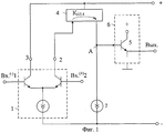
Наиболее близким по сущности к заявляемому техническому решению является классическая схема ОУ фиг.1, представленная в патенте США №4.366.442 fig.1, которая также присутствует в большом числе других патентов, например [1-11], имеющих в качестве цепи нагрузки входных транзисторов управляемые токовые зеркала или неуправляемые токостабилизирующие двухполюсники.The closest in essence to the claimed technical solution is the classical scheme of the
Существенный недостаток известного ОУ фиг.1 состоит в том, что он имеет повышенное значение систематической составляющей напряжения смещения нуля (Uсм), зависящей от свойств его архитектуры.A significant drawback of the known op-amp of FIG. 1 is that it has an increased value of the systematic component of the zero bias voltage (U cm ), which depends on the properties of its architecture.
Основная задача предлагаемого изобретения состоит в уменьшении абсолютного значения Uсм и его температурного и радиационного дрейфа.The main objective of the invention is to reduce the absolute value of U cm and its temperature and radiation drift.
Поставленная задача достигается тем, что в дифференциальном операционном усилителе фиг.1, содержащем входной дифференциальный каскад 1 с первым 2 и вторым 3 токовыми выходами, токовое зеркало 4, вход которого соединен с первым 2 токовым выходом входного дифференциального каскада 1, а выход подключен к базе входного транзистора 5 буферного усилителя 6, токостабилизирующий двухполюсник 7, предусмотрены новые элементы и связи - в схему введены первый 8 и второй 9 дополнительные транзисторы, эмиттеры которых соединены с первым 7 токостабилизирующим двухполюсником, базы являются дополнительными входами 10 и 11 устройства, коллектор первого 8 дополнительного транзистора связан с выходом токового зеркала 4, а эмиттер входного транзистора 5 буферного усилителя 6 связан со вторым 12 дополнительным токостабилизирующим двухполюсником.This object is achieved in that in the differential operational amplifier of figure 1, containing the input
Схема усилителя-прототипа показана на фиг.1. На фиг.2 представлена схема заявляемого устройства в соответствии с п.1, п.2, п.3 и п.4 формулы изобретения. На фиг.3 показан вариант включения входного транзистора 5 буферного усилителя 6 по схеме Дарлингтона.The amplifier circuit of the prototype is shown in figure 1. Figure 2 presents a diagram of the inventive device in accordance with
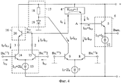
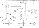
На фиг.4 показана схема ОУ в соответствии с п.5 формулы изобретения, а на фиг.5 и фиг.6 - в соответствии с п.6 формулы изобретения при разных вариантах выполнения первой цепи согласования потенциалов 16.In Fig.4 shows a diagram of the op-amp in accordance with
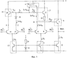
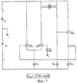
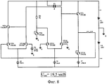
На фиг.7 и фиг.8 показаны схемы дифференциального ОУ-прототипа (фиг.7) и заявляемого ОУ (фиг.8) в среде компьютерного моделирования PSpice на моделях интегральных транзисторов ФГУП НПП «Пульсар».In Fig.7 and Fig.8 shows a diagram of a differential op-amp prototype (Fig.7) and the claimed opamp (Fig.8) in a computer simulation environment PSpice on models of integrated transistors of FSUE NPP Pulsar.
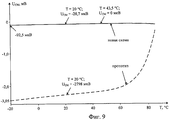
На фиг.9 приведены температурные зависимости напряжения смещения нуля сравниваемых схем фиг.7 и фиг.8.Figure 9 shows the temperature dependence of the zero bias voltage of the compared circuits of Fig.7 and Fig.8.
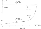
На фиг.10 приведена схема фиг.4 в среде PSpice для случая, когда двухполюсники 13, 14, 12 - резисторы.Figure 10 shows a diagram of figure 4 in the environment of PSpice for the case when the two-
На фиг.11 показана зависимость напряжения смещения нуля Uсм от температуры схем фиг.10 и фиг.7 для случая, когда в схеме фиг.7 - I1=2 МА, I2,=I3=1 МА.In Fig.11 shows the dependence of the bias voltage of zero U cm from the temperature of the circuits of Fig.10 and Fig.7 for the case when in the circuit of Fig.7 - I 1 = 2 MA, I 2, = I 3 = 1 MA.
Дифференциальный операционный усилитель фиг.2 содержит входной дифференциальный каскад 1 с первым 2 и вторым 3 токовыми выходами, токовое зеркало 4, вход которого соединен с первым 2 токовым выходом входного дифференциального каскада 1, а выход подключен к базе входного транзистора 5 буферного усилителя 6, токостабилизирующий двухполюсник 7. В схему введены первый 8 и второй 9 дополнительные транзисторы, эмиттеры которых соединены с первым 7 токостабилизирующим двухполюсником, базы являются дополнительными входами 10 и 11 устройства, коллектор первого 8 дополнительного транзистора связан с выходом токового зеркала 4, а эмиттер входного транзистора 5 буферного усилителя 6 связан со вторым 12 дополнительным токостабилизирующим двухполюсником. Входной дифференциальный каскад 1 выполнен на двухполюснике 13 и транзисторах 14 и 15.The differential operational amplifier of figure 2 contains an input
Кроме этого, на фиг.2, в соответствии с п.3 формулы изобретения, второй 3 токовый выход входного дифференциального каскада 1 связан с первой 16 цепью согласования потенциалов.In addition, in figure 2, in accordance with
На фиг.3, в соответствии с п.2 формулы изобретения, входной транзистор 5 буферного усилителя 6 выполнен в виде составного транзистора Дарлингтона.Figure 3, in accordance with
В соответствии с п.4 формулы изобретения, на фиг.4 коллектор второго 9 дополнительного транзистора связан со второй 17 цепью согласования потенциалов. В частном случае (фиг.4) эта цепь согласования потенциалов содержит резистор 18 и р-n переход 19.In accordance with
На фиг.4, в соответствии с п.5 формулы изобретения, первая 16 цепь согласования потенциалов реализована на основе третьего 20 дополнительного транзистора, эмиттер которого является выходом первой 16 цепи согласования потенциалов, коллектор связан с шиной источника питания, а база соединена со входом токового зеркала 4.In Fig. 4, in accordance with
На фиг.5, в соответствии с п.6 формулы изобретения, вторая 17 цепь согласования потенциалов выполнена на четвертом 21 дополнительном транзисторе, эмиттер которого через вспомогательный резистор 22 связан с выходом второй 17 цепью согласования потенциалов, коллектор подключен к шине источника питания, а база соединена со входом токового зеркала 4.In Fig. 5, in accordance with
На фиг.6 приведена схема ОУ в соответствии с п.6 формулы изобретения, но при другом исполнении первой 16 цепи согласования потенциалов (на основе р-n перехода).Fig.6 shows a diagram of the op-amp in accordance with
Рассмотрим факторы, определяющие систематическую составляющую напряжения смещения нуля Uсм в схеме фиг.2, т.е. зависящие от схемотехники ОУ.Consider the factors that determine the systematic component of the bias voltage of zero U cm in the circuit of figure 2, i.e. circuit-dependent op amps.
Если токи двухполюсников 13 и 7 равны величине 2I0, a двухполюсника 12 - величине I0 (I12=I0), то токи коллекторов транзисторов схемы:If the currents of the two-
![]()
![]()
![]()
![]()
![]()
![]()
где Iб.p=Iэ.i/βi - ток базы n-р-n транзисторов при эмиттерном токеwhere I b.p = I e.i / β i is the base current of n-pn transistors at an emitter current
Iэ.i=I0;I e . I = I 0 ;
βi - коэффициент усиления по току базы транзисторов.β i is the current gain of the base of transistors.
Поэтому разность токов в узле «А» при его коротком замыкании на эквипотенциальную общую шинуTherefore, the current difference in the node "A" when it is shorted to the equipotential common bus
![]()
![]()
где IБУ - ток базы р-n-р транзистора 5.where I BU - base
Для того чтобы получить Iр=0, необходимо, в соответствии с п.2 формулы изобретения, использовать схему фиг.3, для которой IБУ<<Iб.p. В этом случае необходимо также обеспечить за счет первой цепи согласования потенциалов 16 идентичность статических режимов транзисторов 14 и 15, а за счет второй цепи согласования потенциалов 17 - идентичность статических режимов транзисторов 9 и 8 по напряжению коллектор - база.In order to obtain I p = 0, it is necessary, in accordance with
Особенность схемы фиг.4, соответствующей п.5 формулы изобретения, состоит в том, что здесь не должен использоваться в качестве входного транзистора 5 буферного усилителя 6 составной транзистор Дарлингтона фиг.3. Для фиг.4 разностный ток в узле «А» также равен нулю, но при IБУ=Iб.p:A feature of the circuit of FIG. 4 corresponding to
![]()
![]()
В схеме фиг.5, соответствующей п.6 формулы изобретения, идентичный статический режим транзисторов 14 и 15 обеспечивается транзистором 20 и р-n переходом 23, а транзисторов 8 и 9 - транзистором 21 и резистором 22. При этом разностный ток в узле «А»:In the circuit of FIG. 5 corresponding to
![]()
![]()
где Iб.5=2Iб.р - ток базы транзистора 5.where I b.5 = 2I b.r - base current of
Замечательной особенностью схемы фиг.5 является одинаковое построение всех трех токостабилизирующих двухполюсников 13, 7 и 12.A remarkable feature of the circuit of Fig. 5 is the same construction of all three current-stabilizing two-
Для схемы фиг.6, соответствующей п.6 формулы изобретения, разностный ток в узле «А»:For the circuit of Fig.6, corresponding to claim 6 of the claims, the differential current in the node "A":
![]()
![]()
Однако здесь токостабилизирующие двухполюсники 13 и 7, в отличие от двухполюсника 12, имеют другое построение (I13=2I0, I7=2I0, I12=2I0).However, here the current-stabilizing two-
Таким образом, во всех вариантах заявляемого устройства при выполнении условия Ip=0 уменьшается систематическая составляющая Uсм, обусловленная конечной величиной β транзисторов и его радиационной (или температурной) зависимостью. Как следствие, это уменьшает Uсм, так как разностный ток Iр в узле «А» создает Uсм, зависящее от крутизны S преобразования входного дифференциального напряжения uвx в выходной ток узла «А»:Thus, in all variants of the claimed device, when the condition I p = 0 is fulfilled, the systematic component U cm decreases due to the final value of β transistors and its radiation (or temperature) dependence. As a consequence, it reduces the U cm, since a difference current I p at node "A" creates U cm, depending on the steepness S u Bx converting differential input voltage into an output current node "A":
![]()
![]()
где rэ15=rэ14 - сопротивления эмиттерных переходов входных транзисторов 15 и 14 входного дифференциального каскада 1.where r e15 = r e14 - the resistance of the emitter junctions of the
Поэтому для схемы фиг.2Therefore, for the circuit of FIG. 2

где φт=26 мВ - температурный потенциал.where φ t = 26 mV is the temperature potential.
В ОУ-прототипе Ip≠0, поэтому здесь систематическая составляющая Uсм получается как минимум на порядок больше, чем в заявляемой схеме.In the op-amp prototype I p ≠ 0, therefore, here the systematic component U cm is obtained at least an order of magnitude more than in the claimed scheme.
Компьютерное моделирование схем фиг.7 и фиг.8 подтверждает (фиг.9) данные теоретические выводы.Computer simulation of the circuits of Fig.7 and Fig.8 confirms (Fig.9) these theoretical conclusions.
Кроме этого, график фиг.11 показывает, что при использовании резисторов в качестве токостабилизирующих двухполюсников 13, 7 и 12 (фиг.4) заявляемого ОУ также имеет высокую стабильность Uсм.In addition, the graph of FIG. 11 shows that when using resistors as current-stabilizing two-
Несмотря на существенное уменьшение β транзисторов вследствие радиационных воздействий предлагаемый ОУ имеет в этом случае меньшее напряжение смещения нуля, чем ОУ-прототип.Despite a significant decrease in β transistors due to radiation exposure, the proposed op-amp has in this case a lower bias voltage than the op-amp.
Таким образом, заявляемое устройство обладает существенными преимуществами в сравнении с прототипом по величине статической ошибки усиления сигналов постоянного тока. В связи с наличием двух дифференциальных входов его применение достаточно перспективно в радиоэлектронной аппаратуре нового поколения [12, 13].Thus, the claimed device has significant advantages in comparison with the prototype in terms of the value of the static error of amplification of DC signals. Due to the presence of two differential inputs, its use is quite promising in a new generation of electronic equipment [12, 13].
Библиографический списокBibliographic list
1. Патент США №4.415.868 fig.3.1. US Patent No. 4,415,868 fig. 3.
2. Патент ФРГ №2928841 fig.3.2. Germany patent No. 2928841 fig. 3.
3. Патент Японии JP 54-34589 кл. 98 (5) А014.3. Japan patent JP 54-34589 C. 98 (5) A014.
4. Патент Японии JP 154-10221, кл. H03F 3/45.4. Japanese Patent JP 154-10221,
5. Патент Японии JP 54-102949, кл. 98 (5) А21.5. Japan patent JP 54-102949, cl. 98 (5) A21.
6. Патент США №4.366.442 fig.2.6. US Patent No. 4,366,442 fig.2.
7. Патент США №6.426.678.7. US patent No. 6.426.678.
8. Патентная заявка США 2007/0152753 fig.5c.8. US Patent Application 2007/0152753 fig.5c.
9. Патент США №6.531.920, fig.4.9. US Patent No. 6,531,920, fig. 4.
10. Патент США №4.262.261.10. US patent No. 4.262.261.
11. Ежков Ю.А. Справочник по схемотехнике усилителей. - 2-е изд., перераб. - М.: ИП РадиоСофт, 2002. - 272 с. - Рис.9.3 (стр.235).11. Ezhkov Yu.A. Handbook of amplifier circuitry. - 2nd ed., Revised. - M .: IP RadioSoft, 2002 .-- 272 p. - Fig. 9.3 (p. 235).
12. Старченко Е.И. Операционные усилители с мультидифференциальными входными каскадами [Текст]. / Е.И.Старченко. // Проблемы современной аналоговой микросхемотехники: сб. материалов Международного научно-практического семинара: В 2-х ч. Ч.1. - Шахты: Изд-во ЮРГУЭС, 2002 г. - С.35-42.12. Starchenko E.I. Operational amplifiers with multidifferential input stages [Text]. / E.I. Starchenko. // Problems of modern analog microcircuitry: Sat. materials of the International scientific and practical seminar: In 2
13. Крутчинский С.Г. Мультидифференциальные операционные усилители и прецизионная микросхемотехника [Текст]. / С.Г.Крутчинский, Е.И.Старченко. // Международный научно-технический журнал "Электроника и связь". - 2004. - №20. - С.37-45.13. Krutchinsky S.G. Multidifferential operational amplifiers and precision microcircuitry [Text]. / S.G. Krutchinsky, E.I. Starchenko. // International scientific and technical journal "Electronics and Communications". - 2004. - No. 20. - S. 37-45.
Claims (6)
Priority Applications (1)
| Application Number | Priority Date | Filing Date | Title |
|---|---|---|---|
| RU2009133157/09A RU2412535C1 (en) | 2009-09-03 | 2009-09-03 | Differential operating amplifier |
Applications Claiming Priority (1)
| Application Number | Priority Date | Filing Date | Title |
|---|---|---|---|
| RU2009133157/09A RU2412535C1 (en) | 2009-09-03 | 2009-09-03 | Differential operating amplifier |
Publications (1)
| Publication Number | Publication Date |
|---|---|
| RU2412535C1 true RU2412535C1 (en) | 2011-02-20 |
Family
ID=46310205
Family Applications (1)
| Application Number | Title | Priority Date | Filing Date |
|---|---|---|---|
| RU2009133157/09A RU2412535C1 (en) | 2009-09-03 | 2009-09-03 | Differential operating amplifier |
Country Status (1)
| Country | Link |
|---|---|
| RU (1) | RU2412535C1 (en) |
Cited By (4)
| Publication number | Priority date | Publication date | Assignee | Title |
|---|---|---|---|---|
| RU2519348C1 (en) * | 2013-05-14 | 2014-06-10 | Федеральное государственное бюджетное образовательное учреждение высшего профессионального образования "Южно-Российский государственный университет экономики и сервиса" (ФГБОУ ВПО "ЮРГУЭС") | Controlled amplifier and analogue signal mixer based on darlington differential stage |
| RU2523124C1 (en) * | 2013-01-09 | 2014-07-20 | Федеральное государственное бюджетное образовательное учреждение высшего профессионального образования "Южно-Российский государственный университет экономики и сервиса" (ФГБОУ ВПО "ЮРГУЭС") | Multi-differential operational amplifier |
| RU2668985C1 (en) * | 2017-11-09 | 2018-10-05 | федеральное государственное бюджетное образовательное учреждение высшего образования "Донской государственный технический университет" (ДГТУ) | Quick-acting buffer amplifier |
| RU2730911C2 (en) * | 2011-10-10 | 2020-08-26 | Астриум Лимитед | Power amplifier control system |
Citations (3)
| Publication number | Priority date | Publication date | Assignee | Title |
|---|---|---|---|---|
| US3921090A (en) * | 1974-11-14 | 1975-11-18 | Rca Corp | Operational transconductance amplifier |
| US3922614A (en) * | 1973-07-13 | 1975-11-25 | Philips Corp | Amplifier circuit |
| US4366442A (en) * | 1979-09-19 | 1982-12-28 | Tokyo Shibaura Denki Kabushiki Kaisha | Amplifier with muting circuit |
-
2009
- 2009-09-03 RU RU2009133157/09A patent/RU2412535C1/en not_active IP Right Cessation
Patent Citations (3)
| Publication number | Priority date | Publication date | Assignee | Title |
|---|---|---|---|---|
| US3922614A (en) * | 1973-07-13 | 1975-11-25 | Philips Corp | Amplifier circuit |
| US3921090A (en) * | 1974-11-14 | 1975-11-18 | Rca Corp | Operational transconductance amplifier |
| US4366442A (en) * | 1979-09-19 | 1982-12-28 | Tokyo Shibaura Denki Kabushiki Kaisha | Amplifier with muting circuit |
Non-Patent Citations (1)
| Title |
|---|
| ПОЛОННИКОВ Д.Е. Операционные усилители: Принципы построения, теория, схемотехника. - М.: Энергоатомиздат, 1983, с.94, рис.3,9. * |
Cited By (4)
| Publication number | Priority date | Publication date | Assignee | Title |
|---|---|---|---|---|
| RU2730911C2 (en) * | 2011-10-10 | 2020-08-26 | Астриум Лимитед | Power amplifier control system |
| RU2523124C1 (en) * | 2013-01-09 | 2014-07-20 | Федеральное государственное бюджетное образовательное учреждение высшего профессионального образования "Южно-Российский государственный университет экономики и сервиса" (ФГБОУ ВПО "ЮРГУЭС") | Multi-differential operational amplifier |
| RU2519348C1 (en) * | 2013-05-14 | 2014-06-10 | Федеральное государственное бюджетное образовательное учреждение высшего профессионального образования "Южно-Российский государственный университет экономики и сервиса" (ФГБОУ ВПО "ЮРГУЭС") | Controlled amplifier and analogue signal mixer based on darlington differential stage |
| RU2668985C1 (en) * | 2017-11-09 | 2018-10-05 | федеральное государственное бюджетное образовательное учреждение высшего образования "Донской государственный технический университет" (ДГТУ) | Quick-acting buffer amplifier |
Similar Documents
| Publication | Publication Date | Title |
|---|---|---|
| RU2412535C1 (en) | Differential operating amplifier | |
| RU2416155C1 (en) | Differential operating amplifier | |
| RU2416150C1 (en) | Differential operating amplifier | |
| RU2412537C1 (en) | Differential operating amplifier | |
| RU2416149C1 (en) | Differential operating amplifier with low zero offset voltage | |
| RU2412540C1 (en) | Differential operating amplifier | |
| RU2411637C1 (en) | Precision operational amplifier with low voltage of zero shift | |
| RU2412538C1 (en) | Differential operating amplifier | |
| RU2416152C1 (en) | Differential operating amplifier | |
| RU2412539C1 (en) | Differential operating amplifier | |
| RU2444119C1 (en) | Precision operational amplifier | |
| RU2412533C1 (en) | Differential operating amplifier | |
| RU2412534C1 (en) | Differential operating amplifier | |
| RU2411636C1 (en) | Cascode differential amplifier with low voltage of zero shift | |
| RU2416151C1 (en) | Differential operating amplifier | |
| RU2419198C1 (en) | Precision operating amplifier | |
| RU2412532C1 (en) | Differential operating amplifier | |
| RU2408975C1 (en) | Cascode differential amplifier | |
| RU2400925C1 (en) | Differential operating amplifier | |
| RU2416153C1 (en) | Differential operating amplifier | |
| RU2402154C1 (en) | Differential amplifier with low voltage of zero shift | |
| RU2416154C1 (en) | Two-cascade differential amplifier with low supply voltage | |
| RU2595926C1 (en) | Bipolar-field operational amplifier | |
| RU2412528C1 (en) | Cascode differential operating amplifier with low zero offset voltage | |
| RU2568318C1 (en) | Multidifferential operating amplifier with low zero offset voltage |
Legal Events
| Date | Code | Title | Description |
|---|---|---|---|
| MM4A | The patent is invalid due to non-payment of fees |
Effective date: 20130904 |