JP7593557B2 - Low Z-height LED array package with TSV support structure - Google Patents
Low Z-height LED array package with TSV support structure Download PDFInfo
- Publication number
- JP7593557B2 JP7593557B2 JP2023502868A JP2023502868A JP7593557B2 JP 7593557 B2 JP7593557 B2 JP 7593557B2 JP 2023502868 A JP2023502868 A JP 2023502868A JP 2023502868 A JP2023502868 A JP 2023502868A JP 7593557 B2 JP7593557 B2 JP 7593557B2
- Authority
- JP
- Japan
- Prior art keywords
- leds
- redistribution layer
- light
- inorganic substrate
- packaging structure
- Prior art date
- Legal status (The legal status is an assumption and is not a legal conclusion. Google has not performed a legal analysis and makes no representation as to the accuracy of the status listed.)
- Active
Links
Images


Classifications
-
- H—ELECTRICITY
- H10—SEMICONDUCTOR DEVICES; ELECTRIC SOLID-STATE DEVICES NOT OTHERWISE PROVIDED FOR
- H10W—GENERIC PACKAGES, INTERCONNECTIONS, CONNECTORS OR OTHER CONSTRUCTIONAL DETAILS OF DEVICES COVERED BY CLASS H10
- H10W90/00—Package configurations
-
- H—ELECTRICITY
- H10—SEMICONDUCTOR DEVICES; ELECTRIC SOLID-STATE DEVICES NOT OTHERWISE PROVIDED FOR
- H10H—INORGANIC LIGHT-EMITTING SEMICONDUCTOR DEVICES HAVING POTENTIAL BARRIERS
- H10H20/00—Individual inorganic light-emitting semiconductor devices having potential barriers, e.g. light-emitting diodes [LED]
- H10H20/80—Constructional details
- H10H20/81—Bodies
- H10H20/822—Materials of the light-emitting regions
- H10H20/824—Materials of the light-emitting regions comprising only Group III-V materials, e.g. GaP
- H10H20/825—Materials of the light-emitting regions comprising only Group III-V materials, e.g. GaP containing nitrogen, e.g. GaN
-
- H—ELECTRICITY
- H10—SEMICONDUCTOR DEVICES; ELECTRIC SOLID-STATE DEVICES NOT OTHERWISE PROVIDED FOR
- H10H—INORGANIC LIGHT-EMITTING SEMICONDUCTOR DEVICES HAVING POTENTIAL BARRIERS
- H10H20/00—Individual inorganic light-emitting semiconductor devices having potential barriers, e.g. light-emitting diodes [LED]
- H10H20/80—Constructional details
- H10H20/85—Packages
- H10H20/851—Wavelength conversion means
- H10H20/8511—Wavelength conversion means characterised by their material, e.g. binder
- H10H20/8512—Wavelength conversion materials
-
- H—ELECTRICITY
- H10—SEMICONDUCTOR DEVICES; ELECTRIC SOLID-STATE DEVICES NOT OTHERWISE PROVIDED FOR
- H10H—INORGANIC LIGHT-EMITTING SEMICONDUCTOR DEVICES HAVING POTENTIAL BARRIERS
- H10H20/00—Individual inorganic light-emitting semiconductor devices having potential barriers, e.g. light-emitting diodes [LED]
- H10H20/80—Constructional details
- H10H20/85—Packages
- H10H20/855—Optical field-shaping means, e.g. lenses
-
- H—ELECTRICITY
- H10—SEMICONDUCTOR DEVICES; ELECTRIC SOLID-STATE DEVICES NOT OTHERWISE PROVIDED FOR
- H10H—INORGANIC LIGHT-EMITTING SEMICONDUCTOR DEVICES HAVING POTENTIAL BARRIERS
- H10H20/00—Individual inorganic light-emitting semiconductor devices having potential barriers, e.g. light-emitting diodes [LED]
- H10H20/80—Constructional details
- H10H20/85—Packages
- H10H20/857—Interconnections, e.g. lead-frames, bond wires or solder balls
-
- H—ELECTRICITY
- H10—SEMICONDUCTOR DEVICES; ELECTRIC SOLID-STATE DEVICES NOT OTHERWISE PROVIDED FOR
- H10H—INORGANIC LIGHT-EMITTING SEMICONDUCTOR DEVICES HAVING POTENTIAL BARRIERS
- H10H29/00—Integrated devices, or assemblies of multiple devices, comprising at least one light-emitting semiconductor element covered by group H10H20/00
- H10H29/10—Integrated devices comprising at least one light-emitting semiconductor component covered by group H10H20/00
- H10H29/14—Integrated devices comprising at least one light-emitting semiconductor component covered by group H10H20/00 comprising multiple light-emitting semiconductor components
- H10H29/142—Two-dimensional arrangements, e.g. asymmetric LED layout
-
- H—ELECTRICITY
- H10—SEMICONDUCTOR DEVICES; ELECTRIC SOLID-STATE DEVICES NOT OTHERWISE PROVIDED FOR
- H10W—GENERIC PACKAGES, INTERCONNECTIONS, CONNECTORS OR OTHER CONSTRUCTIONAL DETAILS OF DEVICES COVERED BY CLASS H10
- H10W70/00—Package substrates; Interposers; Redistribution layers [RDL]
- H10W70/60—Insulating or insulated package substrates; Interposers; Redistribution layers
- H10W70/611—Insulating or insulated package substrates; Interposers; Redistribution layers for connecting multiple chips together
-
- H—ELECTRICITY
- H10—SEMICONDUCTOR DEVICES; ELECTRIC SOLID-STATE DEVICES NOT OTHERWISE PROVIDED FOR
- H10W—GENERIC PACKAGES, INTERCONNECTIONS, CONNECTORS OR OTHER CONSTRUCTIONAL DETAILS OF DEVICES COVERED BY CLASS H10
- H10W70/00—Package substrates; Interposers; Redistribution layers [RDL]
- H10W70/60—Insulating or insulated package substrates; Interposers; Redistribution layers
- H10W70/62—Insulating or insulated package substrates; Interposers; Redistribution layers characterised by their interconnections
- H10W70/63—Vias, e.g. via plugs
- H10W70/635—Through-vias
-
- H—ELECTRICITY
- H10—SEMICONDUCTOR DEVICES; ELECTRIC SOLID-STATE DEVICES NOT OTHERWISE PROVIDED FOR
- H10W—GENERIC PACKAGES, INTERCONNECTIONS, CONNECTORS OR OTHER CONSTRUCTIONAL DETAILS OF DEVICES COVERED BY CLASS H10
- H10W72/00—Interconnections or connectors in packages
- H10W72/20—Bump connectors, e.g. solder bumps or copper pillars; Dummy bumps; Thermal bumps
-
- H—ELECTRICITY
- H10—SEMICONDUCTOR DEVICES; ELECTRIC SOLID-STATE DEVICES NOT OTHERWISE PROVIDED FOR
- H10W—GENERIC PACKAGES, INTERCONNECTIONS, CONNECTORS OR OTHER CONSTRUCTIONAL DETAILS OF DEVICES COVERED BY CLASS H10
- H10W72/00—Interconnections or connectors in packages
- H10W72/90—Bond pads, in general
-
- F—MECHANICAL ENGINEERING; LIGHTING; HEATING; WEAPONS; BLASTING
- F21—LIGHTING
- F21S—NON-PORTABLE LIGHTING DEVICES; SYSTEMS THEREOF; VEHICLE LIGHTING DEVICES SPECIALLY ADAPTED FOR VEHICLE EXTERIORS
- F21S41/00—Illuminating devices specially adapted for vehicle exteriors, e.g. headlamps
- F21S41/10—Illuminating devices specially adapted for vehicle exteriors, e.g. headlamps characterised by the light source
- F21S41/14—Illuminating devices specially adapted for vehicle exteriors, e.g. headlamps characterised by the light source characterised by the type of light source
- F21S41/141—Light emitting diodes [LED]
-
- F—MECHANICAL ENGINEERING; LIGHTING; HEATING; WEAPONS; BLASTING
- F21—LIGHTING
- F21S—NON-PORTABLE LIGHTING DEVICES; SYSTEMS THEREOF; VEHICLE LIGHTING DEVICES SPECIALLY ADAPTED FOR VEHICLE EXTERIORS
- F21S41/00—Illuminating devices specially adapted for vehicle exteriors, e.g. headlamps
- F21S41/20—Illuminating devices specially adapted for vehicle exteriors, e.g. headlamps characterised by refractors, transparent cover plates, light guides or filters
- F21S41/285—Refractors, transparent cover plates, light guides or filters not provided in groups F21S41/24 - F21S41/2805
-
- G—PHYSICS
- G03—PHOTOGRAPHY; CINEMATOGRAPHY; ANALOGOUS TECHNIQUES USING WAVES OTHER THAN OPTICAL WAVES; ELECTROGRAPHY; HOLOGRAPHY
- G03B—APPARATUS OR ARRANGEMENTS FOR TAKING PHOTOGRAPHS OR FOR PROJECTING OR VIEWING THEM; APPARATUS OR ARRANGEMENTS EMPLOYING ANALOGOUS TECHNIQUES USING WAVES OTHER THAN OPTICAL WAVES; ACCESSORIES THEREFOR
- G03B15/00—Special procedures for taking photographs; Apparatus therefor
- G03B15/02—Illuminating scene
- G03B15/03—Combinations of cameras with lighting apparatus; Flash units
- G03B15/05—Combinations of cameras with electronic flash apparatus; Electronic flash units
-
- G—PHYSICS
- G03—PHOTOGRAPHY; CINEMATOGRAPHY; ANALOGOUS TECHNIQUES USING WAVES OTHER THAN OPTICAL WAVES; ELECTROGRAPHY; HOLOGRAPHY
- G03B—APPARATUS OR ARRANGEMENTS FOR TAKING PHOTOGRAPHS OR FOR PROJECTING OR VIEWING THEM; APPARATUS OR ARRANGEMENTS EMPLOYING ANALOGOUS TECHNIQUES USING WAVES OTHER THAN OPTICAL WAVES; ACCESSORIES THEREFOR
- G03B2215/00—Special procedures for taking photographs; Apparatus therefor
- G03B2215/05—Combinations of cameras with electronic flash units
- G03B2215/0564—Combinations of cameras with electronic flash units characterised by the type of light source
- G03B2215/0567—Solid-state light source, e.g. LED, laser
-
- H—ELECTRICITY
- H10—SEMICONDUCTOR DEVICES; ELECTRIC SOLID-STATE DEVICES NOT OTHERWISE PROVIDED FOR
- H10W—GENERIC PACKAGES, INTERCONNECTIONS, CONNECTORS OR OTHER CONSTRUCTIONAL DETAILS OF DEVICES COVERED BY CLASS H10
- H10W72/00—Interconnections or connectors in packages
- H10W72/20—Bump connectors, e.g. solder bumps or copper pillars; Dummy bumps; Thermal bumps
- H10W72/221—Structures or relative sizes
- H10W72/222—Multilayered bumps, e.g. a coating on top and side surfaces of a bump core
-
- H—ELECTRICITY
- H10—SEMICONDUCTOR DEVICES; ELECTRIC SOLID-STATE DEVICES NOT OTHERWISE PROVIDED FOR
- H10W—GENERIC PACKAGES, INTERCONNECTIONS, CONNECTORS OR OTHER CONSTRUCTIONAL DETAILS OF DEVICES COVERED BY CLASS H10
- H10W72/00—Interconnections or connectors in packages
- H10W72/20—Bump connectors, e.g. solder bumps or copper pillars; Dummy bumps; Thermal bumps
- H10W72/251—Materials
- H10W72/252—Materials comprising solid metals or solid metalloids, e.g. PbSn, Ag or Cu
-
- H—ELECTRICITY
- H10—SEMICONDUCTOR DEVICES; ELECTRIC SOLID-STATE DEVICES NOT OTHERWISE PROVIDED FOR
- H10W—GENERIC PACKAGES, INTERCONNECTIONS, CONNECTORS OR OTHER CONSTRUCTIONAL DETAILS OF DEVICES COVERED BY CLASS H10
- H10W90/00—Package configurations
- H10W90/701—Package configurations characterised by the relative positions of pads or connectors relative to package parts
- H10W90/721—Package configurations characterised by the relative positions of pads or connectors relative to package parts of bump connectors
- H10W90/724—Package configurations characterised by the relative positions of pads or connectors relative to package parts of bump connectors between a chip and a stacked insulating package substrate, interposer or RDL
-
- H—ELECTRICITY
- H10—SEMICONDUCTOR DEVICES; ELECTRIC SOLID-STATE DEVICES NOT OTHERWISE PROVIDED FOR
- H10W—GENERIC PACKAGES, INTERCONNECTIONS, CONNECTORS OR OTHER CONSTRUCTIONAL DETAILS OF DEVICES COVERED BY CLASS H10
- H10W90/00—Package configurations
- H10W90/701—Package configurations characterised by the relative positions of pads or connectors relative to package parts
- H10W90/791—Package configurations characterised by the relative positions of pads or connectors relative to package parts of direct-bonded pads
- H10W90/794—Package configurations characterised by the relative positions of pads or connectors relative to package parts of direct-bonded pads between a chip and a stacked insulating package substrate, interposer or RDL
Landscapes
- Engineering & Computer Science (AREA)
- Physics & Mathematics (AREA)
- General Engineering & Computer Science (AREA)
- General Physics & Mathematics (AREA)
- Microelectronics & Electronic Packaging (AREA)
- Optics & Photonics (AREA)
- Led Device Packages (AREA)
- Semiconductor Lasers (AREA)
Description
本願は、2020年7月15日に出願された米国特許出願第63/052151号及び2020年9月9日に出願された欧州特許出願第20195344.5号に対する優先権を主張し、それらのそれぞれは参照によりその全体が本願に組み込まれている。 This application claims priority to U.S. Patent Application No. 63/052151, filed July 15, 2020, and European Patent Application No. 20195344.5, filed September 9, 2020, each of which is incorporated herein by reference in its entirety.
本開示は、一般に、密集した(densely packed)発光ダイオード又はレーザのための高密度基板の製造に関する。スルーシリコンビア(TSV)を含み、LEDピクセルアレイのアドレスをサポートする電気相互接続システムを説明する。 This disclosure relates generally to the fabrication of high density substrates for densely packed light emitting diodes or lasers. An electrical interconnect system is described that includes through silicon vias (TSVs) to support addressing of LED pixel arrays.
半導体発光デバイス(LED)は、高密度に実装されたグループ又はブロックに配置又は形成できる。しかしながら、発光デバイスが小さいか又は多くの発光デバイスがグループ化される場合、とりわけ、各発光デバイスが個別にアドレス可能であり、適切な熱除去も提供しなければならない場合、信頼性の高い相互接続を提供するのは困難である。 Semiconductor light emitting devices (LEDs) can be arranged or formed in densely packed groups or blocks. However, when the light emitting devices are small or when many light emitting devices are grouped together, it is difficult to provide reliable interconnections, especially when each light emitting device must be individually addressable and adequate heat removal must also be provided.
多数のアドレス可能なピクセルを有するLEDを取り付けるための1つの解決策は、小さな電気的トレース、広範なファンイン若しくはファンアウト構造又はビアを提供する必要がある。これは、例えば、固体セラミック、ガラス又はシリコン基板に個々のLED又はLEDモジュールを取り付けることにより実現できる。残念ながら、そのような取り付けシステムは、高価な材料の使用、多数のマイクロビアの提供及び複雑な処理装置を必要とし得る。また、多くの場合、セラミックの取り付けシステムは、有機回路基板材料に対して乏しいか熱膨張係数(CTE)が整合せず、熱膨張及び収縮サイクルにより早期にトレースの相互接続に障害が生じ、セラミックと有機材料の境界でトレースの破損が起こる。 One solution for mounting LEDs with a large number of addressable pixels requires providing small electrical traces, extensive fan-in or fan-out structures or vias. This can be achieved, for example, by mounting individual LEDs or LED modules to a solid ceramic, glass or silicon substrate. Unfortunately, such mounting systems can require the use of expensive materials, the provision of a large number of microvias, and complex processing equipment. Also, ceramic mounting systems often have poor or mismatched coefficient of thermal expansion (CTE) with organic circuit board materials, causing premature failure of trace interconnects due to thermal expansion and contraction cycles, and trace breakage at the ceramic-organic material interface.
本発明の実施形態によれば、発光体ピクセルアレイ用パッケージング構造は、複数のピクセルであって、少なくとも一部のピクセルはピクセル光閉じ込め構造によって横方向に互いに分離されている、複数のピクセルを含む。上部再配線層を有する無機基板は複数のピクセルに取り付けられ、導電体を含む少なくとも1つのスルーシリコンビアは、無機基板を貫通し、上部再配線層との電気的結合を支持するように画定され、上部再配線層は、該少なくとも1つのスルーシリコンビアと、複数のピクセルとの間に配置されている。 According to an embodiment of the present invention, a packaging structure for a light emitter pixel array includes a plurality of pixels, at least some of which are laterally separated from one another by pixel light confinement structures. An inorganic substrate having a top redistribution layer is attached to the plurality of pixels, and at least one through-silicon via including a conductor is defined through the inorganic substrate to support electrical coupling with the top redistribution layer, the top redistribution layer being disposed between the at least one through-silicon via and the plurality of pixels.
一部の実施形態では、上部再配線層は銅ポストを用いて各ピクセルに取り付けられている。 In some embodiments, the top redistribution layer is attached to each pixel using copper posts.
一部の実施形態では、上部再配線層は前ポストと直接接触し、各ピクセルは、それを銅ポストに取り付けるはんだ材料と直接接触している。 In some embodiments, the top redistribution layer is in direct contact with the front post, and each pixel is in direct contact with the solder material that attaches it to the copper post.
一部の実施形態では、無機基板は、導電体を含む少なくとも1つのスルーシリコンビアに直接接触する底部再配線層をさらに含む。一部の実施形態では、少なくとも1つのスルーシリコンビアは、上部再配線層と、底部再配線層との間にありながら、上部再配線層に直接接触している。 In some embodiments, the inorganic substrate further comprises a bottom redistribution layer in direct contact with at least one through silicon via comprising a conductive material. In some embodiments, the at least one through silicon via is in direct contact with the top redistribution layer while being between the top redistribution layer and the bottom redistribution layer.
一部の実施形態では、光閉じ込め構造は、反射側面コーティングで少なくとも部分的に取り囲まれた蛍光体材料をさらに含む。 In some embodiments, the light containment structure further comprises a phosphor material at least partially surrounded by a reflective side coating.
一部の実施形態では、光閉じ込め構造は、蛍光体材料と整列した拡散層をさらに含む。 In some embodiments, the light containment structure further includes a diffusing layer aligned with the phosphor material.
一部の実施形態では、パッケージング構造の全Z高さは300ミクロン未満である。 In some embodiments, the total Z height of the packaging structure is less than 300 microns.
一部の実施形態では、複数のピクセルは少なくとも9つのピクセルを含む。 In some embodiments, the plurality of pixels includes at least 9 pixels.
一部の実施形態では、複数のピクセルはセグメント化されたGaN層から形成されている。 In some embodiments, the pixels are formed from a segmented GaN layer.
一部の実施形態では、複数のピクセルは、充填トレンチによって分離されたピクセルを有するセグメント化されたGaN層から形成されている。 In some embodiments, the pixels are formed from a segmented GaN layer with the pixels separated by filled trenches.
一部の実施形態では、無機基板の底部再配線層にCMOSダイが取り付けられている。 In some embodiments, the CMOS die is attached to the bottom redistribution layer of the inorganic substrate.
一部の実施形態では、セグメント化されたGaN層と、前記無機基板との間にアンダーフィルが設けられている。 In some embodiments, an underfill is provided between the segmented GaN layer and the inorganic substrate.
一部の実施形態では、無機基板上に回路が形成されている。 In some embodiments, the circuit is formed on an inorganic substrate.
一部の実施形態では、無機基板に少なくとも1つのセンサが取り付けられている。 In some embodiments, at least one sensor is attached to the inorganic substrate.
一部の実施形態では、無機基板に少なくとも1つのセンサ温度センサが取り付けられている。 In some embodiments, at least one sensor temperature sensor is attached to the inorganic substrate.
一部の実施形態では、隣接ピクセルは、ピクセル光閉じ込め構造によって30ミクロン未満で分離されている。 In some embodiments, adjacent pixels are separated by less than 30 microns by pixel light confinement structures.
一部の実施形態では、ピクセル光閉じ込め構造は、シリコーン又はエポキシによって上部再配線層から離隔されている。 In some embodiments, the pixel light confinement structure is separated from the top redistribution layer by silicone or epoxy.
本発明の実施形態によれば、アダプティブ照明システムは、ピクセル光閉じ込め構造によって横方向に互いに分離された隣接ピクセルを有する複数のピクセルであって、該ピクセルのそれぞれは独立して制御可能である、複数のピクセルと、上部再配線層を有し、複数のピクセルに取り付けられる無機基板と、導電体を含み、上部再配線層との電気的結合を支持するために無機基板を貫通するように画定された少なくとも1つのスルーシリコンビアであって、上部再配線層は、該少なくとも1つのスルーシリコンビアと、複数のピクセルとの間に配置されている、少なくとも1つのスルーシリコンビアと、複数のピクセルから離隔され、複数のピクセルによって放射される光を方向付けるレンズと、を含む。 According to an embodiment of the present invention, an adaptive lighting system includes a plurality of pixels having adjacent pixels laterally separated from one another by pixel light confinement structures, each of the pixels being independently controllable; an inorganic substrate having an upper redistribution layer and attached to the plurality of pixels; at least one through silicon via including a conductor and defined through the inorganic substrate to support electrical coupling with the upper redistribution layer, the upper redistribution layer being disposed between the at least one through silicon via and the plurality of pixels; and a lens spaced from the plurality of pixels to direct light emitted by the plurality of pixels.
本発明の実施形態によれば、モバイル装置は、カメラと、フラッシュ照明システムであって、ピクセル光閉じ込め構造によって横方向に互いに分離された隣接ピクセルを有する複数のピクセルと、上部再配線層を有し、複数のピクセルに取り付けられる無機基板と、導電体を含み、上部再配線層との電気的結合を支持するために無機基板を貫通するように画定された少なくとも1つのスルーシリコンビアであって、上部再配線層は、該少なくとも1つのスルーシリコンビアと、複数のピクセルとの間に配置されている、少なくとも1つのスルーシリコンビアと、複数のピクセルから離隔され、複数のピクセルによって放射される光を、カメラの視野内に向かわせるレンズと、を含むフラッシュ照明システムと、を含む。 According to an embodiment of the present invention, a mobile device includes a camera and a flash illumination system including: a plurality of pixels having adjacent pixels laterally separated from one another by pixel light confinement structures; an inorganic substrate having an upper redistribution layer and attached to the plurality of pixels; at least one through silicon via including a conductor and defined through the inorganic substrate to support electrical coupling with the upper redistribution layer, the upper redistribution layer being disposed between the at least one through silicon via and the plurality of pixels; and a lens spaced from the plurality of pixels and configured to direct light emitted by the plurality of pixels into a field of view of the camera.
以下の図面を参照しながら、本開示の非限定的及び非網羅的な実施形態を説明する。以下の図面において、同様の参照符号は、特に明記されていない限り、様々な図面の全体にわたって同様の部分を表す。
以下の詳細な説明は、図面を参照しながら読むべきである。図面において、ことなる図面全体を通して同じ参照符号は同様の要素を表す。必ずしも縮尺通りではない図面は、選択的な実施形態を示し、本発明の範囲を制限することを意図していない。詳細な説明は発明の原理を限定的ではなく、一例として示す。 The following detailed description should be read with reference to the drawings, in which like reference characters represent like elements throughout the different drawings. The drawings, which are not necessarily to scale, depict selective embodiments and are not intended to limit the scope of the invention. The detailed description illustrates by way of example, but not by way of limitation, principles of the invention.
図1は、基板1040に配置された発光半導体ダイオード(LED)構造1020と、LEDに配置された蛍光体層1060とを含む個々のpcLED1000の一例を示す。発光半導体ダイオード構造1020は、n型及びp型層の間に配置される活性領域を通常含む。ダイオード構造にわたって適切な順方向バイアスを適用することで、活性領域から光の放射がもたらされる。放射光の波長は、活性領域の組成及び構造によって決定される。
Figure 1 shows an example of an
LEDは、例えば、紫外線、青色、緑色又は赤色光を放出するIII族窒化物LEDであり得る。任意の他の適切な材料システムから形成され、任意の他の適切な波長の光を放射するLEDを用いてもよい。他の適切な材料システムは、例えば、III-リン化物材料、III-ヒ化物材料及びII-VI材料を含み得る。 The LEDs may be, for example, III-nitride LEDs that emit ultraviolet, blue, green, or red light. LEDs formed from any other suitable material systems and emitting light at any other suitable wavelengths may also be used. Other suitable material systems may include, for example, III-phosphide materials, III-arsenide materials, and II-VI materials.
pcLEDからの望ましい光出力及び色の仕様に応じて、任意の適切な蛍光体材料が用いられ得る。 Any suitable phosphor material may be used depending on the desired light output and color specifications from the pcLED.
図2A及び図2Bは、基板2020に配置された蛍光体ピクセル1060を含むpcLED1000のアレイ2000の断面図及び上面図をそれぞれ示す。このようなアレイは、任意の適切な方法で配置された任意の適切な数のpcLEDを含み得る。図示の例では、アレイは共有の基板上にモノリシックに形成されるものとして記載されているが、代替的に、pcLEDのアレイは個別のpcLEDから形成され得る。基板2020は、LEDを駆動するためのCMOS回路を任意で含んでもよく、任意の適切な材料で形成され得る。
2A and 2B show cross-sectional and top views, respectively, of an
図2A及び2Bは、9個のpcLEDの3×3のアレイを示すが、そのようなアレイは、例えば、数十個、数百個、数千個のLEDを含み得る。個々のLED(ピクセル)は、アレイの平面内に幅(例えば、辺の長さ)を有し、例えば、1ミリメートル(mm)以下、500ミクロン以下、100ミクロン以下又は50ミクロン以下であり得る。そのようなアレイ内のLEDは、アレイの平面内に、例えば、数百ミクロン、100ミクロン以下、50ミクロン以下、10ミクロン以下又は5ミクロン以下の幅を有する道又はレーンによって、互いに離隔され得る。図の例は、対称的なマトリックスに配置された矩形のピクセルを示すが、ピクセル及びアレイは、任意の適切な形状又は配置を有していてもよい。 2A and 2B show a 3×3 array of 9 pcLEDs, but such an array may include, for example, tens, hundreds, or thousands of LEDs. Individual LEDs (pixels) have a width (e.g., side length) in the plane of the array, which may be, for example, 1 millimeter (mm) or less, 500 microns or less, 100 microns or less, or 50 microns or less. LEDs in such an array may be separated from one another by paths or lanes having a width in the plane of the array, for example, hundreds of microns, 100 microns or less, 50 microns or less, 10 microns or less, or 5 microns or less. Although the illustrated example shows rectangular pixels arranged in a symmetrical matrix, the pixels and arrays may have any suitable shape or arrangement.
アレイの平面内に約50ミクロン以下の寸法(例えば、辺長)を有するLEDは、マイクロLEDと通常呼ばれ、そのようなマイクロLEDのアレイは、マイクロLEDアレイと呼ばれ得る。 LEDs having dimensions (e.g., side lengths) of about 50 microns or less in the plane of the array are typically referred to as micro-LEDs, and an array of such micro-LEDs may be referred to as a micro-LED array.
LEDのアレイ又はそのようなアレイの一部は、個別のLEDピクセルがトレンチ及び/又は絶縁材料によって互いに電気的に遮蔽されているが、電気的に遮蔽されたセグメントは半導体構造の部分によって互いに物理的に接続されたままである、セグメント化されたモノリシック構造として形成され得る。 An array of LEDs, or a portion of such an array, may be formed as a segmented monolithic structure in which individual LED pixels are electrically shielded from one another by trenches and/or insulating materials, but the electrically shielded segments remain physically connected to one another by portions of the semiconductor structure.
LEDアレイ内の個別のLEDは、個別にアドレス可能であり得るか、アレイ内のピクセルのグループ又はサブセットの一部としてアドレス可能であり得るか又はアドレス可能でない場合がある。そのため、発光体ピクセルアレイは、光の分布のきめ細い強度、空間的及び時間的制御を必要とするか又はそのような制御の恩恵を受けるあらゆる用途に有用である。これらの用途は、限定されないが、ピクセルブロック又は個別のピクセルからの放射光の正確な特殊パターニングを含み得る。用途に応じて、放射光はスペクトル的に区別され、経時的に適応し及び/又は環境に応答し得る。そのような発光体ピクセルアレイは、さまざまな強度、空間的又は時間的なパターンで予めプログラムされた光の分布を提供し得る。放射光は、受信されたセンサデータに少なくとも部分的に基づいてもいいし、光無線通信のために用いられ得る。関連するエレクトロニクス及び光学は、ピクセル、ピクセルブロック又はデバイスレベルで異なり得る。 Individual LEDs in an LED array may be individually addressable, addressable as part of a group or subset of pixels in the array, or non-addressable. Emitter pixel arrays are thus useful for any application that requires or benefits from fine intensity, spatial and temporal control of light distribution. These applications may include, but are not limited to, precise specialized patterning of emitted light from pixel blocks or individual pixels. Depending on the application, the emitted light may be spectrally differentiated, adaptive over time, and/or responsive to the environment. Such emitter pixel arrays may provide pre-programmed distributions of light with different intensity, spatial or temporal patterns. The emitted light may be based at least in part on received sensor data or may be used for optical wireless communication. The associated electronics and optics may vary at the pixel, pixel block, or device level.
図3A~図3Bに示すように、pcLEDアレイ2000は、電源及び制御モジュール3020、センサモジュール3040及びLED取り付け領域3060を含む電子基板3000に取り付けられ得る。電源及び制御モジュール3020は、外部ソースからの電力及び制御信号と、センサモジュール3040からの信号とを受信し、電源及び制御モジュール3020は、これらの信号に基づいて、LEDの動作を制御する。センサモジュール3040は、任意の適切なセンサ、例えば温度又は光センサから信号を受信し得る。あるいは、pcLEDアレイ2000は、電源及び制御モジュールと、センサモジュールとは別の基板(図示せず)に取り付けられてもよい。
As shown in Figures 3A-3B, the
個別のpcLEDは、任意で、蛍光体層に配置されるか又は隣接して位置するレンズ又は他の光学素子を包含し得るか又は組み合わせで配置され得る。図示しないこのような光学素子は、「一次光学素子」と呼ばれ得る。加えて、図4A~図4Bに示すように、(例えば、電子基板3000に取り付けられる)pcLEDアレイ2000は、意図する用途で用いられる、導波管、レンズ又はその両方等の二次光学素子との組み合わせで配置され得る。図4Aでは、pcLED1000によって放射される光は導波管4020によって収集され、投影レンズ4040に向けられる。投影レンズ4040は、例えば、フレネルレンズであり得る。この配置は、例えば、自動車のヘッドライトでの使用に好適であり得る。図4Bでは、pcLED1000によって放射された光は、介在する導波管を用いずに投影レンズ4040によって直接収集される。この配置は、pcLEDが互いに十分に近い間隔で配置できる場合にとりわけ好適であり、自動車のヘッドライトに加えてカメラのフラッシュ用途でも用いられ得る。マイクロLEDディスプレイ用途は、例えば図4A~図4Bに示すものと同様の光学配置を用いり得る。一般に、所望の用途に応じて、光学素子の任意の適切な配置を、本明細書で説明するLEDアレイと組み合わせて用いられ得る。
Individual pcLEDs may optionally include or be arranged in combination with lenses or other optical elements disposed on or adjacent to the phosphor layer. Such optical elements, not shown, may be referred to as "primary optical elements." In addition, as shown in Figures 4A-4B, the pcLED array 2000 (e.g., mounted on an electronic board 3000) may be arranged in combination with secondary optical elements, such as a waveguide, a lens, or both, used in the intended application. In Figure 4A, light emitted by the
特定の目的に適応可能な照明を提供するために、独立して動作可能なLEDのアレイがレンズ、レンズシステム又は他の光学系(例えば、上記したもの)と組み合わせて用いられ得る。例えば、動作の際、そのようなアダプティブ照明システムは、照明されたシーン又はオブジェクトにわたって色及び/又は強度が変化する及び/又は所望の方向に向けられる照明を提供し得る。コントローラは、シーン内のオブジェクト又は人の位置及び色の特性を示すデータを受信し、その情報に基づいて、シーンに適応された照明を提供するためにLEDアレイ内のLEDを制御するように構成され得る。そのようなデータは、例えば、画像センサ又は光学(例えば、レーザ走査)又は非光学(例えば、ミリレーダ)センサにより提供できる。このようなアダプティブな照明は、自動車、モバイルデバイスカメラ、VR及びARの用途にとってますます重要になっている。 Arrays of independently operable LEDs may be used in combination with lenses, lens systems, or other optical systems (e.g., as described above) to provide lighting that is adaptable to a particular purpose. For example, in operation, such adaptive lighting systems may provide lighting that varies in color and/or intensity across an illuminated scene or object and/or is directed in a desired direction. A controller may be configured to receive data indicative of the location and color characteristics of objects or people in a scene and, based on that information, control the LEDs in the LED array to provide lighting adapted to the scene. Such data may be provided, for example, by image sensors or optical (e.g., laser scanning) or non-optical (e.g., millimeter radar) sensors. Such adaptive lighting is becoming increasingly important for automotive, mobile device camera, VR and AR applications.
図5は、上述したシステムと同様又は同一であり得るLEDアレイ及びレンズシステム5020を含む例示のカメラフラッシュシステム5000を概略的に示す。フラッシュシステム5000は、マイクロプロセッサ等のコントローラ5040によって制御されるLEDドライバ5060も含む。コントローラ5040は、カメラ5070及びセンサ5080にも結合され、メモリ5100に記憶された命令及びプロファイルに従って動作し得る。カメラ5070及びアダプティブ照明システム5020は、それらの視野を一致させるためにコントローラ5040によって制御され得る。
Figure 5 shows a schematic of an example
センサ5080は、例えば、位置センサ(例えば、ジャイロスコープ及び/又は加速度計)及び/又はシステム5000の位置、速度及び向きを特定するために用いられ得る他のセンサを含み得る。センサ5080からの信号は、コントローラ5040の適切な一連の行動(例えば、どのLEDがターゲットを現在照らしているか、どのLEDが所定の時間の後にターゲットを照らすか)を決定するためにコントローラ5040に供給され得る。
The
動作中、5020内のLEDアレイの一部又は全てのピクセルからの照明は、調整-動作停止されるか、最大強度で運転されるか又は中間強度で運転され得る。5020内のLEDアレイによって放射された光のビームフォーカス又はステアリングは、照明装置内の光学系を動かすか又はレンズのフォーカスを変更することなく、ビームの形状を動的に調整できるようにするために、ピクセルのうちの1つ以上のサブセットを作動させることにより電子的に行うことができる。 During operation, illumination from some or all of the pixels of the LED array in 5020 can be adjusted-deactivated, operated at full intensity, or operated at intermediate intensity. Beam focusing or steering of the light emitted by the LED array in 5020 can be done electronically by activating one or more subsets of the pixels to allow dynamic adjustment of the shape of the beam without moving optics or changing the focus of lenses in the illumination device.
図6に見られるように、断面図に示す発光体ピクセルアレイ100のパッケージング構造は、CMOSダイ及び支持体104に任意で取り付けることができるマルチピクセルアセンブリ102を含む。一実施形態では、ピクセルアセンブリ102は、蛍光体及びディフューザ層122が取り付けられたGaN又は他の適切なアクティブ発光体120を含む。個別のピクセルは、ピクセル光閉じ込め構造124によって分離されている。アクティブ発光体120及び蛍光体/ディフューザ122は、導電性材料が充填されたスルーシリコンビア(TSV)を有するシリコン基板130を用いて、支持及び電気的に結合(例えば、直接電気的に接続)することができる。一実施形態では、銅又は他の金属ポスト140を、はんだ材料142で発光体120に取り付けることができる。電気的に非導電性で接着性のアンダーフィル132を活用して、銅ピラー140を保護し、発光体120をシリコン基板130に取り付けることができる。銅ピラー140は、シリコン基板130の上面に形成又は塗布された導電性の上部再配線層144に取り付けることができる。上部再配線層144は、スルーシリコンビア(TSV)146内の導電性材料に電気的に結合(例えば、直接電気的に接続)されている。TSV146は、シリコン基板130の底面に形成又は塗布された導電性底部再配線層148に接続されている。この高密度の電気接続スキームは、ピクセル又はピクセルのグループが個別にアドレスされ、光の強度について制御できるようにするため有利である。一部の実施形態では、マルチピクセルアセンブリ102の厚さ(Z高さ)は500ミクロン以下である。一部の実施形態では、マルチピクセルアセンブリ102の厚さは300ミクロン以下である。一部の実施形態では、厚さは250~300ミクロンである。一部の実施形態では、マルチピクセルアセンブリ102の厚さは250ミクロン以下である。一部の実施形態では、厚さは100~300ミクロンである。 As seen in FIG. 6, the packaging structure of the emitter pixel array 100 shown in cross section includes a multi-pixel assembly 102 that can be optionally attached to a CMOS die and a support 104. In one embodiment, the pixel assembly 102 includes a GaN or other suitable active emitter 120 with a phosphor and diffuser layer 122 attached. Individual pixels are separated by pixel light confinement structures 124. The active emitter 120 and phosphor/diffuser 122 can be supported and electrically coupled (e.g., directly electrically connected) using a silicon substrate 130 with through-silicon vias (TSVs) filled with a conductive material. In one embodiment, copper or other metal posts 140 can be attached to the emitters 120 with a solder material 142. An electrically non-conductive, adhesive underfill 132 can be utilized to protect the copper pillars 140 and attach the emitters 120 to the silicon substrate 130. The copper pillars 140 may be attached to a conductive top redistribution layer 144 formed or applied to the top surface of the silicon substrate 130. The top redistribution layer 144 is electrically coupled (e.g., directly electrically connected) to conductive material in through silicon vias (TSVs) 146. The TSVs 146 are connected to a conductive bottom redistribution layer 148 formed or applied to the bottom surface of the silicon substrate 130. This high density electrical connection scheme is advantageous because it allows pixels or groups of pixels to be individually addressed and controlled for light intensity. In some embodiments, the thickness (Z height) of the multi-pixel assembly 102 is 500 microns or less. In some embodiments, the thickness of the multi-pixel assembly 102 is 300 microns or less. In some embodiments, the thickness is between 250 and 300 microns. In some embodiments, the thickness of the multi-pixel assembly 102 is 250 microns or less. In some embodiments, the thickness is between 100 and 300 microns.
説明した構造及びシステムには様々な利点がある。発光素子用にシリコン基板を用いることで、アダプティブライティングシステムに高密度の相互接続が提供されるのと同時に、有機基板に比べて良好な熱伝達特性を提供する。また、薄くてかさばらないライティングモジュールのために低Z高さのパッケージが必要である。とりわけ、単純なLEDフラッシュ照明システムと同様の高さを有することで、従来の非ピクセルのカメラフラッシュをアドレス可能なアダプティブフラッシュに簡単に再設計し且つ置き換えることができる。 The described structure and system have various advantages. The use of silicon substrates for the light emitting elements provides high density interconnects for the adaptive lighting system while at the same time providing better heat transfer properties compared to organic substrates. Also, a low Z height package is required for a thin and non-bulky lighting module. Notably, having a similar height to a simple LED flash illumination system allows for easy redesign and replacement of conventional non-pixelated camera flashes with addressable adaptive flashes.
マルチピクセルアセンブリ102は、様々な種類、サイズ及びレイアウトの発光素子を含むことができる。一実施形態では、個別にアドレス可能な発光ダイオード(LED)の一又は二次元マトリックスアレイを用いることができる。個別にアドレス可能なLEDのN×Mアレイ(N及びMはそれぞれ1~2000)を用いることができる。3×3のアレイ又は7×7のアレイ等の、個別にアドレス可能なLEDのN×Mアレイ(N及びMはそれぞれ3~9)を用いることができる。個別のLED構造は、LEDの発光面の平面を見た場合に、正方形、長方形、六角形、多角形、円形、円弧又は他の表面形状を有することができる。LEDアセンブリ又は構造のアレイは、幾何学的に真っすぐな行及び列、互い違いの行又は列、曲線又は半ランダム若しくはランダムなレイアウトで配置できる。LEDアセンブリは、個別にアドレス可能なピクセルアレイとして形成された複数のLEDを含むことができる。一部の実施形態では、LEDへの導電線の放射状又は他の非矩形のグリッド配列を含めることができる。一部の実施形態では、LEDへの導電線の曲線、巻線、ヘビ状及び/又は他の適切な非線形配列を含めることができる。 The multi-pixel assembly 102 can include light emitting elements of various types, sizes, and layouts. In one embodiment, a one or two dimensional matrix array of individually addressable light emitting diodes (LEDs) can be used. An N×M array of individually addressable LEDs (N and M each are 1-2000) can be used. An N×M array of individually addressable LEDs (N and M each are 3-9), such as a 3×3 array or a 7×7 array, can be used. The individual LED structures can have a square, rectangular, hexagonal, polygonal, circular, arcuate, or other surface shape when viewed in the plane of the LED's light emitting surface. The array of LED assemblies or structures can be geometrically arranged in straight rows and columns, staggered rows or columns, curved, or semi-random or random layouts. The LED assembly can include multiple LEDs formed as an individually addressable pixel array. Some embodiments can include a radial or other non-rectangular grid arrangement of conductive lines to the LEDs. Some embodiments can include curved, wound, serpentine, and/or other suitable non-linear arrangement of conductive lines to the LEDs.
幅広い色を提供するために、様々な蛍光体及び関連するディフューザ122を用いることができる。ディフューザは、フィルム、コーティング又はポリマーバインダ若しくは他の適切な材料に分散した酸化チタンを含むことができる。ディフューザに加えて、LED構造体は、成形又はセラミック蛍光体等の波長変換材料又は量子ドット若しくはダイ等の他の材料で覆うことができる。複数の種類及び厚さの蛍光体を用いることができる。1つ以上の波長変換材料と組み合わせたLEDが、白色光又は他の色の単色光を作り出すために用いられ得る。LEDによって放射された光の全て又は一部のみが波長変換材料によって変換され得る。変換されていない光は、最終的な光のスペクトルの一部であり得るが、必ずしもそうでなくてよい。一般的なデバイスの例としては、黄色発光蛍光体と組み合わされた青色発光LED、緑及び赤色発光蛍光体と組み合わされた青色発光LED、青色及び黄色発光蛍光体と組み合わされたUV発光LED、青色、緑色及び赤色発光蛍光体と組み合わされたUV発光LEDを含む。蛍光体は、電圧の印加によりLED上に電気泳動的に堆積できる。印加電圧の期間を変化させると、それに対応して堆積される蛍光体の量及び厚さが変化する。あるいは、蛍光体粒子をLEDに付着させるために有機バインダを用いて、LEDを蛍光体でコーティングできる。蛍光体及び/又はディフューザ材料は、分注、スクリーン印刷、噴霧、成形、フィルムとして塗布又はラミネートできる。あるいは、特定の用途では、ガラスに含まれる蛍光体又は予め成形された焼結セラミック蛍光体をLEDに取り付けることができる。一部の実施形態では、蛍光体及び関連するディフューザ122の厚さ(Z高さ)は200ミクロン以下である。一部の実施形態では、蛍光体及び関連するディフューザ122の厚さは50~110ミクロンである。蛍光体及び関連するディフューザ122内の蛍光体層の厚さは60ミクロン以下であってもよく、各セグメントがLED幅に一致する幅を有するシリコーン内のセグメント化された蛍光体であり得る。蛍光体及び関連するディフューザ122内のディフューザ要素は、5~45ミクロン等の5~100ミクロンの厚さを有し得る。ディフューザ要素は、酸化チタン又は酸化チタンと共にバインダ要素内に分散された酸化アルミニウムであり得る。バインダ要素内に分散された酸化チタン又は酸化アルミニウムは、0.01重量%~3重量%、例えば0.6重量%の濃度を有し得る。 A variety of phosphors and associated diffusers 122 can be used to provide a wide range of colors. Diffusers can include titanium oxide films, coatings, or dispersed in a polymer binder or other suitable material. In addition to the diffuser, the LED structure can be coated with a wavelength conversion material such as a molded or ceramic phosphor or other material such as quantum dots or dies. Multiple types and thicknesses of phosphors can be used. LEDs combined with one or more wavelength conversion materials can be used to create white light or other colored monochromatic light. All or only a portion of the light emitted by the LED can be converted by the wavelength conversion material. The unconverted light can be, but is not necessarily, part of the final light spectrum. Examples of common devices include a blue-emitting LED combined with a yellow-emitting phosphor, a blue-emitting LED combined with a green- and red-emitting phosphor, a UV-emitting LED combined with a blue- and yellow-emitting phosphor, and a UV-emitting LED combined with a blue-, green-, and red-emitting phosphor. The phosphor can be electrophoretically deposited on the LED by application of a voltage. Varying the duration of the applied voltage will correspondingly vary the amount and thickness of phosphor deposited. Alternatively, the LED can be coated with phosphor using an organic binder to adhere the phosphor particles to the LED. The phosphor and/or diffuser material can be dispensed, screen printed, sprayed, molded, applied as a film or laminated. Alternatively, phosphor in glass or preformed sintered ceramic phosphor can be attached to the LED in certain applications. In some embodiments, the thickness (Z height) of the phosphor and associated diffuser 122 is 200 microns or less. In some embodiments, the thickness of the phosphor and associated diffuser 122 is 50-110 microns. The phosphor layer in the phosphor and associated diffuser 122 may be 60 microns or less in thickness and may be a segmented phosphor in silicone with each segment having a width matching the LED width. The diffuser elements in the phosphor and associated diffuser 122 may have a thickness of 5-100 microns, such as 5-45 microns. The diffuser element can be titanium oxide or aluminum oxide dispersed in a binder element with titanium oxide. The titanium oxide or aluminum oxide dispersed in the binder element can have a concentration of 0.01% to 3% by weight, for example 0.6% by weight.
ピクセル光閉じ込め構造124は、光反射性又は光吸収性の側壁コーティングであり得る。これは、追加の光吸収体、反射体(側壁用の分布型ブラッグ反射体を形成する誘電体層のスタックを含む)、他の光学コーティング又は電気絶縁材料を含むか又は有することができる。1つ以上の有機、無機又は有機/無機バインダ及び充填剤材料を含むことができる、光分離及び電気的遮蔽誘電材料を用いることができる。例えば、接着剤、エポキシ、アクリレート又はニトロセルロースを、セラミック又は光吸収若しくは散乱粒子と組み合わせて用いることができる。別の有機/無機バインダ、充填剤又は側壁は、例えば、反射性酸化チタン又は他の反射/散乱粒子が埋め込まれたエポキシであり得る。ピクセル光閉じ込め構造124は、60重量%の酸化チタンを含むシリコーン中の酸化チタンであり得る。無機バインダは、ゾルゲル(例えば、TEOS又はMTMSのゾルゲル)又は水ガラスとしても知られる液体ガラス(例えば、ケイ酸ナトリウム又はケイ酸カリウム)を含むことができる。一部の実施形態では、バインダは物理的特性を調整する充填剤を含むことができる。充填剤は、無機ナノ粒子、シリカ、ガラス粒子若しくはファイバ又は光学若しくは熱的性能を改善できる他の材料を含むことができる。一部の実施形態では、ピクセル光閉じ込め構造124は、30ミクロン以下、例えば20ミクロンの幅を有するように配置される。一部の実施形態では、ピクセル間の距離は30~5ミクロンである。 The pixel light confinement structure 124 may be a light reflective or light absorbing sidewall coating. It may include or have additional light absorbers, reflectors (including a stack of dielectric layers forming a distributed Bragg reflector for the sidewall), other optical coatings or electrically insulating materials. Light isolating and electrically shielding dielectric materials may be used, which may include one or more organic, inorganic or organic/inorganic binders and filler materials. For example, glues, epoxies, acrylates or nitrocellulose may be used in combination with ceramics or light absorbing or scattering particles. Another organic/inorganic binder, filler or sidewall may be, for example, an epoxy embedded with reflective titanium oxide or other reflective/scattering particles. The pixel light confinement structure 124 may be titanium oxide in silicone with 60% titanium oxide by weight. The inorganic binder may include sol-gels (e.g., TEOS or MTMS sol-gels) or liquid glasses, also known as water glasses (e.g., sodium silicate or potassium silicate). In some embodiments, the binder may include fillers to adjust the physical properties. The filler may include inorganic nanoparticles, silica, glass particles or fibers, or other materials that may improve optical or thermal performance. In some embodiments, the pixel light confinement structures 124 are arranged to have a width of 30 microns or less, for example 20 microns. In some embodiments, the distance between pixels is between 30 and 5 microns.
一部の実施形態では、高輝度発光デバイスを形成可能な半導体材料からアクティブ発光体120を形成することができ、限定されないが、III-V族半導体、特に、III-窒化物材料とも呼ばれるガリウム、アルミニウム、インジウム及び窒素の二元、三元、及び四元合金を含むことができる。このような半導体材料は、必要に応じてLED及びレーザーシステムの両方をサポートするように成長させることができる。一部の実施形態では、薄化又は全体若しくは部分的に除去できるサファイア基板を用いることができる。一部の実施形態では、LEDダイをさらに薄化できる。一部の実施形態では、レーザリフトオフ技術によって取り除かれるサファイア基板上に成長させたGaNが用いられる。一部の実施形態では、GaNを全体的に又は部分的にピクセル又はピクセルのグループに分けることができる(例えば、トレンチを定義するために部分的に切り抜く)。一部の実施形態では、アクティブ発光体120の厚さ(Z高さ)は15ミクロン以下である。一部の実施形態では、アクティブ発光体120の厚さは15~7ミクロンになるように選択される。 In some embodiments, the active light emitter 120 can be formed from semiconductor materials capable of forming high brightness light emitting devices, including but not limited to III-V semiconductors, particularly binary, ternary, and quaternary alloys of gallium, aluminum, indium, and nitrogen, also referred to as III-nitride materials. Such semiconductor materials can be grown to support both LED and laser systems as needed. In some embodiments, a sapphire substrate can be used that can be thinned or removed in whole or in part. In some embodiments, the LED die can be further thinned. In some embodiments, GaN grown on a sapphire substrate is used that is removed by laser lift-off techniques. In some embodiments, the GaN can be separated in whole or in part into pixels or groups of pixels (e.g., cut out in parts to define trenches). In some embodiments, the thickness (Z height) of the active light emitter 120 is 15 microns or less. In some embodiments, the thickness of the active light emitter 120 is selected to be between 15 and 7 microns.
一部の実施形態では、銅又は他の金属ポスト140を、はんだ材料142で発光体120に取り付けることができる。例えば、銅又は他の金属ポスト140は、幅が40ミクロン以下で、ピッチが80ミクロン以下のSnAg(スズ銀)のはんだキャップを有する銅からなる銅ピラーを含み得る。一部の実施形態では、バンプオントレース、ACF又はCu-Cu直接接合を用いることができる。一部の実施形態では、金属ポスト140及びはんだ又は他の電気コネクタの厚さ(Z高さ)の合計は60ミクロン以下である。一部の実施形態では、金属ポスト140及びはんだ又は他の電気コネクタの厚さの合計は10~60ミクロンである。 In some embodiments, copper or other metal posts 140 can be attached to the light emitter 120 with solder material 142. For example, the copper or other metal posts 140 can include copper pillars with widths of 40 microns or less and SnAg (tin silver) solder caps with pitches of 80 microns or less. In some embodiments, bump-on-trace, ACF, or Cu-Cu direct bonding can be used. In some embodiments, the sum of the thickness (Z height) of the metal posts 140 and the solder or other electrical connector is 60 microns or less. In some embodiments, the sum of the thickness of the metal posts 140 and the solder or other electrical connector is 10-60 microns.
シリコン基板130は、全体的にシリコンからなり得る。一部の実施形態では、シリコン基板130はシリコンに加えて、有機又は無機基板材料であり得る他の材料を含むことができる。シリコン基板は、取り付けられたCMOSダイ及びLED120のたえのインターポーザであり得る。シリコン基板は、限定されないが、従来のプリント基板を含む、周囲の無機又は有機基板に埋め込むか又は配置できる。一部の実施形態では、シリコン基板は、ガラス、セラミック又は他の無機材料を追加で含むか又は完全に置き換えることができる。一部の実施形態では、基板130の厚さ(Z高さ)は100ミクロン以下である。一部の実施形態では、基板130の厚さは40~100ミクロンである。したがって、基板を貫通するTSV146の厚さ(Z高さ)は100ミクロン以下、例えば、40~100ミクロンであり得る。TSV146は、1:10のアスペクト比を有し、5~10ミクロンの直径を有し得る。例えば、TSV146の直径が10ミクロンの場合、その厚さは100ミクロンであり得る。 The silicon substrate 130 may be entirely made of silicon. In some embodiments, the silicon substrate 130 may include other materials in addition to silicon, which may be organic or inorganic substrate materials. The silicon substrate may be an interposer for the attached CMOS die and LEDs 120. The silicon substrate may be embedded or placed in a surrounding inorganic or organic substrate, including but not limited to a conventional printed circuit board. In some embodiments, the silicon substrate may additionally include or completely replace glass, ceramic, or other inorganic materials. In some embodiments, the thickness (Z height) of the substrate 130 is 100 microns or less. In some embodiments, the thickness of the substrate 130 is between 40 and 100 microns. Thus, the thickness (Z height) of the TSV 146 through the substrate may be 100 microns or less, for example, between 40 and 100 microns. The TSV 146 may have an aspect ratio of 1:10 and a diameter of 5 to 10 microns. For example, if the diameter of the TSV 146 is 10 microns, then the thickness may be 100 microns.
基板130は、基板130の上部、底部、側面及び/又は内部に、導電性上部再配線層144及び底部再配線層148を含む様々な導電性構造を支持することができる。内部導電構造は、基板130において定義された導電性ビアから形成できる。これらの導電性ビアは、導電性ビアに接続するために電気トレースを水平に延ばす上部及び底部再配線層に電気的に接続(例えば、直接電気的に接続)することができる。一部の実施形態では、導電性ビアは、マイクロビア、ワイヤ、金属ピラー、はんだカラム又は他の適切な構造であり得る。理解されるように、ファンイン、ファンアウト、直線状又は曲線状の水平レイアウトを含む、再配線層を形成する電気トレースの様々な配置を利用できる。導電性構造又はトレースは、銅、銀、アルミニウム、金、金属合金又は導電性高分子組成物、グラフェン又は導電性セラミック等の様々な導電性金属から形成できる。一部の実施形態では、コーティング、注入、成形、又は他の適切な適用技術を通じて適用されるアンダーフィル(例えば、シリコーン又はエポキシ)の使用は、不要な電気相互接続のリスクを低減しながら、少なくともいくつかの環境保護も提供できる。 The substrate 130 can support various conductive structures, including a conductive top redistribution layer 144 and a bottom redistribution layer 148, on the top, bottom, sides, and/or interior of the substrate 130. The interior conductive structures can be formed from conductive vias defined in the substrate 130. These conductive vias can be electrically connected (e.g., directly electrically connected) to the top and bottom redistribution layers that extend electrical traces horizontally to connect to the conductive vias. In some embodiments, the conductive vias can be microvias, wires, metal pillars, solder columns, or other suitable structures. As will be appreciated, various arrangements of electrical traces forming the redistribution layers can be utilized, including fan-in, fan-out, linear or curved horizontal layouts. The conductive structures or traces can be formed from various conductive metals, such as copper, silver, aluminum, gold, metal alloys or conductive polymer compositions, graphene, or conductive ceramics. In some embodiments, the use of an underfill (e.g., silicone or epoxy) applied through coating, pouring, molding, or other suitable application technique can also provide at least some environmental protection while reducing the risk of unwanted electrical interconnects.
導電性構造は、適切な電力及び駆動回路に直接接続するか又は追加のプリント基板若しくは他のLEDモジュールシステムを介して接続できる。この電力及び駆動回路は、底部再配線層148を任意のCMOSダイ及び支持体104に接続することにより提供できる。一部の実施形態では、基板130の底部再配線層148と、CMOS及び支持体104上の導体パッドの合計厚さ(Z高さ)は25ミクロン以下である。一部の実施形態では、基板130の底部再配線層148と、CMOS及び支持体104上の導体パッドの合計厚さは25ミクロン以下である。 The conductive structures can be connected directly to appropriate power and drive circuitry or through an additional printed circuit board or other LED module system. This power and drive circuitry can be provided by connecting the bottom redistribution layer 148 to any CMOS die and support 104. In some embodiments, the combined thickness (Z height) of the bottom redistribution layer 148 of the substrate 130 and the CMOS and conductor pads on the support 104 is 25 microns or less. In some embodiments, the combined thickness of the bottom redistribution layer 148 of the substrate 130 and the CMOS and conductor pads on the support 104 is 25 microns or less.
一部の実施形態では、シリコン基板130の底部に熱伝導体(例えば、銅又は他の金属スラグ)を取り付けることができる。一部の実施形態では、マルチピクセルアセンブリ102の横又は近くに配置されたCMOSダイ又は制御回路に接続された導体パッド及び電気トレースを備えた任意のプリント回路基板を用いることができる。 In some embodiments, a thermal conductor (e.g., a copper or other metal slug) can be attached to the bottom of the silicon substrate 130. In some embodiments, any printed circuit board with conductor pads and electrical traces connected to the CMOS die or control circuitry located next to or near the multi-pixel assembly 102 can be used.
一部の実施形態では、マイクロレンズ又は他の一次又は二次光学素子(反射体、散乱体又は吸収体を含む)を、各LEDピクセル及び関連する蛍光体に対して取り付けられ得るか又は配置され得る。他の実施形態では、一次光学素子をLEDのアレイ全体にわたって配置でき、LEDから離れて、適切なパッケージで直接取り付け又は取り付けることができる。保護層、透明層、熱層又は他のパッケージング構造は、特定の用途のために必要に応じて用いることができる。 In some embodiments, microlenses or other primary or secondary optical elements (including reflectors, scatterers or absorbers) may be attached or positioned relative to each LED pixel and associated phosphor. In other embodiments, primary optical elements may be positioned over the entire array of LEDs and may be directly attached or mounted separate from the LEDs in suitable packaging. Protective layers, transparent layers, thermal layers or other packaging structures may be used as needed for a particular application.
図7は、無機又は有機であり得る基板212上で組み立てられたマルチピクセルアセンブリ210を含むシステム200を示す。蛍光体214は、CMOSダイ、制御回路、又はセンサ216をサポートできる周辺領域を含む基板212の中心に置かれている。例えば、一実施形態では、センサ216は、マルチピクセルアセンブリ210の動作を能動的に監視及び制御するために、1つ以上の光、色、加速度又は温度センサを含むことができる。図示のように、一実施形態では、マルチピクセルアセンブリ210は、フレキシブルプリント回路基板220に取り付けることができる。このプリント回路基板220は、追加のピクセルアセンブリ210のための複数の取り付け位置222をさらに含むことができる。マルチピクセルアセンブリ210は、上述の発光体ピクセルアレイ100に対応し、蛍光体214は蛍光体及びディフューザ層122に対応し、基板212は、センサ216が基板130上に配置されるように基板130に対応する要素を含む。
7 shows a
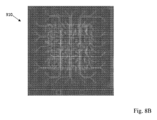
図8A及び8Bは、スルーシリコンビア基板の底部接続及び内部接続をそれぞれ示す。シリコン貫通ビア及び内部再配線層を用いることで、前と後ろの間の複雑な接続スキームをサポートできる。スルーシリコンビア内に配置された銅に接続するトレースを有する底部再配線層300(図6の底部再配線層148に対応)を図8Aに示す。一部の実施形態では、シリコンビア(図1のTSV146に対応)は、例えばグリッド内の等距離の行及び列に沿って、互いに等しく離隔されている。シリコンビア間の間隔は50ミクロン以上、例えば、50~100ミクロン、50~80ミクロン又は50~60ミクロンであり得る。シリコンビアに接続されるトレースは、グリッドの中心に向かって高密度に配置され、グリッドの外側部に向かって低密度に配置されている。図8Bは、TSV基板との接続性310、例えば、上部再配線層310(図6の上部再配線層144に対応)のトレースを示す。トレースは、ピクセルを含む領域の外側にあるシリコンビアに接続するために、ピクセルを含む領域を越えて延び得る。すなわち、一部のシリコンビアの一部及び一部のトレースの部分は、ピクセルのいずれとも重ならなくてもよい。
8A and 8B show the bottom and internal connections of the through silicon via substrate, respectively. Complex connection schemes between the front and back can be supported by using through silicon vias and internal redistribution layers. A bottom redistribution layer 300 (corresponding to bottom redistribution layer 148 of FIG. 6) is shown in FIG. 8A with traces connecting to copper disposed in the through silicon vias. In some embodiments, the silicon vias (corresponding to TSVs 146 of FIG. 1) are equally spaced from each other, for example along equidistant rows and columns in a grid. The spacing between the silicon vias can be 50 microns or more, for example 50-100 microns, 50-80 microns, or 50-60 microns. The traces connecting to the silicon vias are densely arranged toward the center of the grid and sparsely arranged toward the outer portions of the grid. FIG. 8B shows the
説明した様々な実施形態は、光の分布のきめ細かい強度、空間的及び時間的制御の恩恵を受ける用途をサポートし得る発光ピクセルアレイ(すなわち、アドレス可能なLEDアセンブリ)をサポートする。これは、限定されないが、ピクセルブロック又は個別のピクセルからの放射光の正確な空間パターニングを含む。用途に応じて、放射光はスペクトル的に区別され、経時的に適応され及び/又は環境的に応答し得る。発光ピクセルアレイは、様々な強度、空間又は時間パターンで予めプログラムされた光の分布を提供し得る。放射光は、受信されたセンサデータに少なくとも部分的に基づいてもよく、光無線通信のために用いられ得る。関連する光学系は、ピクセル、ピクセルブロック又はデバイスレベルで異なり得る。例示の発光ピクセルアレイは、関連する共通の光学系を有する高輝度ピクセルの共通制御中央ブロックを有するデバイスを含み得る一方で、エッジピクセルは個別の光学系を有し得る。発光ピクセルアレイによってサポートされる一般的な用途は、カメラフラッシュ、自動車のヘッドライト、建築及びエリア照明、街路照明及び情報ディスプレイを含む。 The various embodiments described support light-emitting pixel arrays (i.e., addressable LED assemblies) that can support applications that benefit from fine-grained intensity, spatial, and temporal control of light distribution. This includes, but is not limited to, precise spatial patterning of emitted light from pixel blocks or individual pixels. Depending on the application, the emitted light can be spectrally differentiated, adaptive over time, and/or environmentally responsive. The light-emitting pixel arrays can provide pre-programmed distributions of light with different intensity, spatial, or temporal patterns. The emitted light may be based at least in part on received sensor data and can be used for optical wireless communication. The associated optics can vary at the pixel, pixel block, or device level. An exemplary light-emitting pixel array can include a device with a commonly controlled central block of high-brightness pixels with associated common optics, while edge pixels can have separate optics. Common applications supported by light-emitting pixel arrays include camera flashes, automotive headlights, architectural and area lighting, street lighting, and information displays.
発光ピクセルアレイは、モバイル装置用のカメラフラッシュ用途に適し得る。通常、高輝度LEDからの強力で短いフラッシュ光が画像の取り込みをサポートするために用いられる。残念ながら、従来のLEDフラッシュでは、光の多くは、すでに十分に照らされているか又は照らす必要がない領域の照明に浪費される。発光ピクセルアレイの使用により、シーンの一部に制御された照明を決まった期間にわたって提供され得る。これにより、カメラフラッシュは、例えば、ローリングシャッター撮影の間に撮像される領域のみを照らすか、取り込まれた画像にわたって信号対ノイズ比を最小限に抑え、人又はターゲットの被写体上若しくは被写体にわたる影を最小限に抑える照明を提供し、及び/又は影を強調する高コントラストの照明を提供し得る。発光ピクセルアレイのピクセルのスペクトルが異なる場合、フラッシュ照明の色温度は、必要な色調又は暖かさを提供するために動的に調整され得る。 The light-emitting pixel array may be suitable for camera flash applications for mobile devices. Typically, a strong, short flash of light from a high-brightness LED is used to support image capture. Unfortunately, with a conventional LED flash, much of the light is wasted on illuminating areas that are already well lit or do not need to be lit. The use of a light-emitting pixel array may provide controlled illumination of a portion of a scene for a period of time. This may allow the camera flash to, for example, illuminate only the area being imaged during rolling shutter photography, minimize signal-to-noise ratio across the captured image, provide illumination that minimizes shadows on or across a person or target subject, and/or provide high-contrast illumination that accentuates shadows. If the pixels of the light-emitting pixel array have different spectra, the color temperature of the flash illumination may be dynamically adjusted to provide the required tone or warmth.
道路の選択された部分のみをアクティブに照らす自動車のヘッドライトも、発光ピクセルアレイによってサポートされる。赤外線カメラをセンサとして用いることで、発光ピクセルアレイは道路を照らすために必要なピクセルのみを有効にしながら、歩行者又は対向車の運転手の目をくらませ得るピクセルを無効にする。加えて、運転手の環境意識を改善するために、オフロードの歩行者、動物又は標識が選択的に照らされ得る。発光ピクセルアレイのピクセルのスペクトルが異なる場合、日中、夕暮れ又は夜間の条件のそれぞれに従って光の色温度が調整され得る。一部のピクセルは、光無線車両間通信のために用いられ得る。 Automotive headlights that actively illuminate only selected portions of the road are also supported by emissive pixel arrays. Using an infrared camera as a sensor, the emissive pixel array enables only the pixels necessary to illuminate the road while disabling pixels that may blind pedestrians or oncoming drivers. In addition, off-road pedestrians, animals or signs may be selectively illuminated to improve the driver's environmental awareness. If the pixels of the emissive pixel array have different spectra, the color temperature of the light may be adjusted according to day, twilight or night conditions, respectively. Some pixels may be used for optical wireless vehicle-to-vehicle communication.
建築及び領域照明も、発光ピクセルアレイの恩恵を受け得る。発光ピクセルアレイは、視覚的な表示を改善するか又は照明コストを削減するために、建物又は領域を選択的且つ適応的に照らすために用いられ得る。加えて、発光ピクセルアレイは、装飾的な動き又はビデオ効果のためにメディアファサードを投影するために用いられ得る。追跡センサ及び/又はカメラと組み合わせて、歩行者の周囲の領域の選択的な照明が可能となり得る。照明の色温度を調整することに加えて、波長固有の園芸照明をサポートするために、スペクトルが異なるピクセルが用いられ得る。 Architectural and area lighting may also benefit from light-emitting pixel arrays. Light-emitting pixel arrays may be used to selectively and adaptively illuminate buildings or areas to improve visual display or reduce lighting costs. In addition, light-emitting pixel arrays may be used to project media facades for decorative motion or video effects. In combination with tracking sensors and/or cameras, selective illumination of areas around pedestrians may be possible. In addition to adjusting the color temperature of the lighting, spectrally distinct pixels may be used to support wavelength-specific horticultural lighting.
街路照明は、発光ピクセルアレイの使用から大きな恩恵が得られ得る重要な用途である。様々な街路灯のタイプを模倣するために単一タイプの発光アレイが用いられ、例えば、選択されたピクセルの適切に有効又は無効にすることにより、タイプI直線街路灯とタイプIV半円形街路灯との間での切り替えができる。加えて、環境条件又は使用時間に応じて光ビームの強度又は分布を調整することにより、街路灯のコストが下がり得る。例えば、歩行者がいない場合には、光の強度及び分布領域が低減され得る。発光ピクセルアレイのピクセルのスペクトルが異なる場合、日中、夕暮れ又は夜間の条件のそれぞれに従って光の色温度が調整され得る。 Street lighting is an important application that can greatly benefit from the use of light-emitting pixel arrays. A single type of light-emitting array can be used to mimic different street light types, for example switching between a Type I linear street light and a Type IV semicircular street light by appropriately enabling or disabling selected pixels. In addition, the cost of the street light can be reduced by adjusting the intensity or distribution of the light beam depending on the environmental conditions or time of use. For example, in the absence of pedestrians, the light intensity and distribution area can be reduced. If the pixels of the light-emitting pixel array have different spectra, the color temperature of the light can be adjusted according to day, dusk or night conditions, respectively.
発光アレイは、直接又は投影ディスプレイを必要とする用途をサポートするのにも適している。例えば、警告、緊急又は情報標識は全て、発光アレイを用いて表示又は投影され得る。これは、例えば色が変化するか又は点滅する出口標識の投影を可能にする。発光アレイが多数のピクセルで構成されている場合、テキスト又は数字の情報が提示され得る。方向矢印又は同様の標識も提供され得る。 Light emitting arrays are also suitable to support applications requiring direct or projected displays. For example, warning, emergency or information signs can all be displayed or projected using light emitting arrays. This allows for the projection of color changing or flashing exit signs, for example. If the light emitting array is made up of a large number of pixels, text or numeric information can be presented. Directional arrows or similar signs can also be provided.
本発明を詳細に説明してきたが、当業者であれば、本開示を所与として、本明細書で説明した発明概念の精神から逸脱することなく、本発明に変更が加えられ得ることを理解するであろう。したがって、本発明の範囲を、図示及び説明した特定の実施形態に限定することを意図していない。
Although the invention has been described in detail, those skilled in the art will appreciate, given this disclosure, that modifications may be made to the present invention without departing from the spirit of the inventive concepts described herein. Accordingly, it is not intended that the scope of the invention be limited to the specific embodiments illustrated and described.
Claims (28)
ピクセル状に配置され且つ独立して制御可能な複数の発光ダイオード(LED)を含むセグメント化された一体構造と、
上部再配線層を有し、前記複数のLEDに取り付けられる無機基板と、
導電体を含み、前記上部再配線層との電気的結合を支持するために前記無機基板を貫通するように画定された少なくとも1つのスルービアであって、前記上部再配線層は、該少なくとも1つのスルービアと、前記複数のLEDとの間に配置されている、少なくとも1つのスルービアと、
前記無機基板が配置される支持体と、
前記支持体上にあるセンサと、
を含む、パッケージング構造。 1. A packaging structure for a light emitter pixel array, comprising:
a segmented monolithic structure including a plurality of pixelated, independently controllable light emitting diodes (LEDs);
an inorganic substrate having a top redistribution layer and attached to the plurality of LEDs;
at least one through-via including a conductor and defined through the inorganic substrate to support an electrical coupling with the upper redistribution layer, the upper redistribution layer being disposed between the at least one through-via and the plurality of LEDs;
A support on which the inorganic substrate is placed;
a sensor on the support;
A packaging structure comprising:
上部再配線層を有し、前記複数のLEDに取り付けられる無機基板と、
導電体を含み、前記上部再配線層との電気的結合を支持するために前記無機基板を貫通するように画定された少なくとも1つのスルービアであって、前記上部再配線層は、該少なくとも1つのスルービアと、前記複数のLEDとの間に配置されている、少なくとも1つのスルービアと、
前記少なくとも1つのスルービアに電気的結合されたCMOSと、
を含むアダプティブ照明システム。 A plurality of light emitting diodes (LEDs) arranged in a pixel pattern;
an inorganic substrate having a top redistribution layer and attached to the plurality of LEDs;
at least one through-via including a conductor and defined through the inorganic substrate to support an electrical coupling with the upper redistribution layer, the upper redistribution layer being disposed between the at least one through-via and the plurality of LEDs;
a CMOS electrically coupled to the at least one through via;
Adaptive lighting system including
フラッシュ照明システムであって、
ピクセル状に配置された複数の発光ダイオード(LED)と、
上部再配線層を有し、前記複数のLEDに取り付けられる無機基板と、
導電体を含み、前記上部再配線層との電気的結合を支持するために前記無機基板を貫通するように画定された少なくとも1つのスルービアであって、前記上部再配線層は、該少なくとも1つのスルービアと、前記複数のLEDとの間に配置されている、少なくとも1つのスルービアと、
前記少なくとも1つのスルービアに電気結合されたCMOSと、
前記複数のLEDから離隔され、前記複数のLEDによって放射される光を、前記カメラの視野内に向かわせるように配置されたレンズと、
を含むフラッシュ照明システムと、
を含むモバイル装置。 A camera and
1. A flash illumination system comprising:
A plurality of light emitting diodes (LEDs) arranged in a pixel pattern;
an inorganic substrate having a top redistribution layer and attached to the plurality of LEDs;
at least one through-via including a conductor and defined through the inorganic substrate to support an electrical coupling with the upper redistribution layer, the upper redistribution layer being disposed between the at least one through-via and the plurality of LEDs;
a CMOS electrically coupled to the at least one through via;
a lens spaced from the LEDs and positioned to direct light emitted by the LEDs into a field of view of the camera;
a flash illumination system including:
A mobile device including:
Applications Claiming Priority (5)
| Application Number | Priority Date | Filing Date | Title |
|---|---|---|---|
| US202063052151P | 2020-07-15 | 2020-07-15 | |
| US63/052,151 | 2020-07-15 | ||
| EP20195344.5A EP3968373A1 (en) | 2020-09-09 | 2020-09-09 | Low z-height led array package having tsv support structure |
| EP20195344.5 | 2020-09-09 | ||
| PCT/US2021/041867 WO2022016004A1 (en) | 2020-07-15 | 2021-07-15 | Low z-height led array package having tsv support structure |
Publications (2)
| Publication Number | Publication Date |
|---|---|
| JP2023534276A JP2023534276A (en) | 2023-08-08 |
| JP7593557B2 true JP7593557B2 (en) | 2024-12-03 |
Family
ID=79556067
Family Applications (1)
| Application Number | Title | Priority Date | Filing Date |
|---|---|---|---|
| JP2023502868A Active JP7593557B2 (en) | 2020-07-15 | 2021-07-15 | Low Z-height LED array package with TSV support structure |
Country Status (6)
| Country | Link |
|---|---|
| US (2) | US20230154911A1 (en) |
| EP (1) | EP4182970A4 (en) |
| JP (1) | JP7593557B2 (en) |
| KR (1) | KR102889513B1 (en) |
| CN (1) | CN116114062A (en) |
| WO (1) | WO2022016004A1 (en) |
Families Citing this family (5)
| Publication number | Priority date | Publication date | Assignee | Title |
|---|---|---|---|---|
| CN116114062A (en) | 2020-07-15 | 2023-05-12 | 亮锐有限责任公司 | Low Z height LED array package with TSV support structure |
| JP7510820B2 (en) * | 2020-08-31 | 2024-07-04 | シャープ福山レーザー株式会社 | Image display element |
| WO2023249985A1 (en) * | 2022-06-24 | 2023-12-28 | Lumileds Llc | Engineered scattering in led encapsulants for tunable optical far-field response |
| DE102023111267A1 (en) * | 2023-05-02 | 2024-11-07 | Ams-Osram International Gmbh | METHOD FOR PRODUCING AN OPTOELECTRONIC COMPONENT AND OPTOELECTRONIC COMPONENT |
| KR102922138B1 (en) * | 2025-07-23 | 2026-02-04 | 나노화인테크 주식회사 | Circular Mo Nanogrid Sample Support with Dual Si Post Structures on Upper and Lower Sides |
Citations (5)
| Publication number | Priority date | Publication date | Assignee | Title |
|---|---|---|---|---|
| WO2011108664A1 (en) | 2010-03-03 | 2011-09-09 | 有限会社Mtec | Optical semiconductor device |
| US20170345802A1 (en) | 2016-05-31 | 2017-11-30 | Lg Electronics Inc. | Display device using semiconductor light emitting device and fabrication method thereof |
| WO2019126728A1 (en) | 2017-12-22 | 2019-06-27 | Lumileds Llc | Iii-nitride multi-wavelength light emitting diodes |
| WO2019133628A1 (en) | 2017-12-29 | 2019-07-04 | Lumileds Llc | High density interconnect for segmented leds |
| US20200212100A1 (en) | 2018-12-31 | 2020-07-02 | Lumileds Holdings B.V. | Pixelated led array with optical elements |
Family Cites Families (22)
| Publication number | Priority date | Publication date | Assignee | Title |
|---|---|---|---|---|
| US8563331B2 (en) * | 2005-06-03 | 2013-10-22 | E. I. Du Pont De Nemours And Company | Process for fabricating and repairing an electronic device |
| DE102007059133B4 (en) * | 2007-12-07 | 2023-04-06 | OSRAM Opto Semiconductors Gesellschaft mit beschränkter Haftung | Substrate for an LED submount, LED submount and LED light source |
| US7928655B2 (en) * | 2008-11-10 | 2011-04-19 | Visera Technologies Company Limited | Light-emitting diode device and method for fabricating the same |
| US8535961B1 (en) * | 2010-12-09 | 2013-09-17 | Amkor Technology, Inc. | Light emitting diode (LED) package and method |
| US8653542B2 (en) * | 2011-01-13 | 2014-02-18 | Tsmc Solid State Lighting Ltd. | Micro-interconnects for light-emitting diodes |
| JP5450680B2 (en) * | 2012-02-01 | 2014-03-26 | スタンレー電気株式会社 | Semiconductor light emitting device |
| US9484325B2 (en) | 2013-10-09 | 2016-11-01 | Invensas Corporation | Interconnections for a substrate associated with a backside reveal |
| US10665578B2 (en) | 2015-09-24 | 2020-05-26 | Apple Inc. | Display with embedded pixel driver chips |
| US10037981B2 (en) * | 2016-05-18 | 2018-07-31 | Globalfoundries Inc. | Integrated display system with multi-color light emitting diodes (LEDs) |
| KR101968527B1 (en) * | 2016-05-31 | 2019-04-12 | 엘지전자 주식회사 | Display device using semiconductor light emitting device and method for manufacturing |
| US10400958B2 (en) * | 2016-12-30 | 2019-09-03 | Lumileds Llc | Addressable color changeable LED structure |
| US10770440B2 (en) | 2017-03-15 | 2020-09-08 | Globalfoundries Inc. | Micro-LED display assembly |
| SG11201909518YA (en) | 2017-04-13 | 2019-11-28 | Hong Kong Beida Jade Bird Display Ltd | Led-oled hybrid self-emissive display |
| US10734363B2 (en) | 2017-08-03 | 2020-08-04 | Cree, Inc. | High density pixelated-LED chips and chip array devices |
| US10665560B2 (en) | 2017-10-27 | 2020-05-26 | Taiwan Semiconductor Manufacturing Company Ltd. | Optical semiconductor package and method for manufacturing the same |
| US11054112B2 (en) | 2017-12-22 | 2021-07-06 | Lumileds Llc | Ceramic phosphor with lateral light barriers |
| WO2019132963A1 (en) * | 2017-12-29 | 2019-07-04 | Intel Corporation | Quantum computing assemblies |
| KR102536269B1 (en) * | 2018-09-14 | 2023-05-25 | 삼성전자주식회사 | semiconductor package and method for manufacturing the same |
| JP2020085960A (en) * | 2018-11-16 | 2020-06-04 | 株式会社ブイ・テクノロジー | Full-color led display panel |
| US20230003649A1 (en) | 2019-11-25 | 2023-01-05 | Surgvision Gmbh | Testing of luminescence imaging apparatus with automatic detection of a testing device |
| CN116114062A (en) | 2020-07-15 | 2023-05-12 | 亮锐有限责任公司 | Low Z height LED array package with TSV support structure |
| EP3968373A1 (en) | 2020-09-09 | 2022-03-16 | Lumileds LLC | Low z-height led array package having tsv support structure |
-
2021
- 2021-07-15 CN CN202180063030.5A patent/CN116114062A/en active Pending
- 2021-07-15 KR KR1020237005357A patent/KR102889513B1/en active Active
- 2021-07-15 WO PCT/US2021/041867 patent/WO2022016004A1/en not_active Ceased
- 2021-07-15 JP JP2023502868A patent/JP7593557B2/en active Active
- 2021-07-15 EP EP21841329.2A patent/EP4182970A4/en active Pending
-
2023
- 2023-01-17 US US18/097,939 patent/US20230154911A1/en active Pending
- 2023-01-17 US US18/097,932 patent/US12550788B2/en active Active
Patent Citations (5)
| Publication number | Priority date | Publication date | Assignee | Title |
|---|---|---|---|---|
| WO2011108664A1 (en) | 2010-03-03 | 2011-09-09 | 有限会社Mtec | Optical semiconductor device |
| US20170345802A1 (en) | 2016-05-31 | 2017-11-30 | Lg Electronics Inc. | Display device using semiconductor light emitting device and fabrication method thereof |
| WO2019126728A1 (en) | 2017-12-22 | 2019-06-27 | Lumileds Llc | Iii-nitride multi-wavelength light emitting diodes |
| WO2019133628A1 (en) | 2017-12-29 | 2019-07-04 | Lumileds Llc | High density interconnect for segmented leds |
| US20200212100A1 (en) | 2018-12-31 | 2020-07-02 | Lumileds Holdings B.V. | Pixelated led array with optical elements |
Also Published As
| Publication number | Publication date |
|---|---|
| US20230154911A1 (en) | 2023-05-18 |
| EP4182970A1 (en) | 2023-05-24 |
| JP2023534276A (en) | 2023-08-08 |
| CN116114062A (en) | 2023-05-12 |
| WO2022016004A1 (en) | 2022-01-20 |
| US12550788B2 (en) | 2026-02-10 |
| US20230170456A1 (en) | 2023-06-01 |
| EP4182970A4 (en) | 2024-08-07 |
| KR102889513B1 (en) | 2025-11-24 |
| KR20230039705A (en) | 2023-03-21 |
Similar Documents
| Publication | Publication Date | Title |
|---|---|---|
| JP7593557B2 (en) | Low Z-height LED array package with TSV support structure | |
| US11610935B2 (en) | Fan-out light-emitting diode (LED) device substrate with embedded backplane, lighting system and method of manufacture | |
| JP6992073B2 (en) | How to make a light emitting device | |
| TWI767124B (en) | Led systems, apparatuses, and methods | |
| US11621173B2 (en) | Fan out structure for light-emitting diode (LED) device and lighting system | |
| JP7702066B2 (en) | Flip-chip interconnected light-emitting diode package assembly | |
| EP3968373A1 (en) | Low z-height led array package having tsv support structure | |
| KR102954590B1 (en) | Method for manufacturing a fan-out light-emitting diode (LED) device substrate with an embedded backplane | |
| JP2023535909A (en) | Light emitting device with metal inlay and top contact | |
| EP4634983A1 (en) | Multi-die package with shaped luminance | |
| JP2023536241A (en) | Light emitting device with metal inlay and top contact |
Legal Events
| Date | Code | Title | Description |
|---|---|---|---|
| A521 | Request for written amendment filed |
Free format text: JAPANESE INTERMEDIATE CODE: A523 Effective date: 20230310 |
|
| A621 | Written request for application examination |
Free format text: JAPANESE INTERMEDIATE CODE: A621 Effective date: 20230310 |
|
| A977 | Report on retrieval |
Free format text: JAPANESE INTERMEDIATE CODE: A971007 Effective date: 20240126 |
|
| A131 | Notification of reasons for refusal |
Free format text: JAPANESE INTERMEDIATE CODE: A131 Effective date: 20240206 |
|
| A521 | Request for written amendment filed |
Free format text: JAPANESE INTERMEDIATE CODE: A523 Effective date: 20240417 |
|
| A131 | Notification of reasons for refusal |
Free format text: JAPANESE INTERMEDIATE CODE: A131 Effective date: 20240806 |
|
| A521 | Request for written amendment filed |
Free format text: JAPANESE INTERMEDIATE CODE: A523 Effective date: 20241017 |
|
| TRDD | Decision of grant or rejection written | ||
| A01 | Written decision to grant a patent or to grant a registration (utility model) |
Free format text: JAPANESE INTERMEDIATE CODE: A01 Effective date: 20241022 |
|
| A61 | First payment of annual fees (during grant procedure) |
Free format text: JAPANESE INTERMEDIATE CODE: A61 Effective date: 20241107 |
|
| R150 | Certificate of patent or registration of utility model |
Ref document number: 7593557 Country of ref document: JP Free format text: JAPANESE INTERMEDIATE CODE: R150 |