JP7185548B2 - high frequency amplifier circuit - Google Patents
high frequency amplifier circuit Download PDFInfo
- Publication number
- JP7185548B2 JP7185548B2 JP2019020729A JP2019020729A JP7185548B2 JP 7185548 B2 JP7185548 B2 JP 7185548B2 JP 2019020729 A JP2019020729 A JP 2019020729A JP 2019020729 A JP2019020729 A JP 2019020729A JP 7185548 B2 JP7185548 B2 JP 7185548B2
- Authority
- JP
- Japan
- Prior art keywords
- transistor
- amplifier circuit
- circuit
- output
- output mode
- Prior art date
- Legal status (The legal status is an assumption and is not a legal conclusion. Google has not performed a legal analysis and makes no representation as to the accuracy of the status listed.)
- Active
Links
Images


Classifications
-
- H—ELECTRICITY
- H03—ELECTRONIC CIRCUITRY
- H03F—AMPLIFIERS
- H03F3/00—Amplifiers with only discharge tubes or only semiconductor devices as amplifying elements
- H03F3/26—Push-pull amplifiers; Phase-splitters therefor
- H03F3/265—Push-pull amplifiers; Phase-splitters therefor with field-effect transistors only
-
- H—ELECTRICITY
- H03—ELECTRONIC CIRCUITRY
- H03F—AMPLIFIERS
- H03F3/00—Amplifiers with only discharge tubes or only semiconductor devices as amplifying elements
- H03F3/189—High-frequency amplifiers, e.g. radio frequency amplifiers
-
- H—ELECTRICITY
- H02—GENERATION; CONVERSION OR DISTRIBUTION OF ELECTRIC POWER
- H02P—CONTROL OR REGULATION OF ELECTRIC MOTORS, ELECTRIC GENERATORS OR DYNAMO-ELECTRIC CONVERTERS; CONTROLLING TRANSFORMERS, REACTORS OR CHOKE COILS
- H02P29/00—Arrangements for regulating or controlling electric motors, appropriate for both AC and DC motors
- H02P29/40—Regulating or controlling the amount of current drawn or delivered by the motor for controlling the mechanical load
-
- H—ELECTRICITY
- H03—ELECTRONIC CIRCUITRY
- H03F—AMPLIFIERS
- H03F1/00—Details of amplifiers with only discharge tubes, only semiconductor devices or only unspecified devices as amplifying elements
- H03F1/02—Modifications of amplifiers to raise the efficiency, e.g. gliding Class A stages, use of an auxiliary oscillation
- H03F1/0205—Modifications of amplifiers to raise the efficiency, e.g. gliding Class A stages, use of an auxiliary oscillation in transistor amplifiers
- H03F1/0277—Selecting one or more amplifiers from a plurality of amplifiers
-
- H—ELECTRICITY
- H03—ELECTRONIC CIRCUITRY
- H03F—AMPLIFIERS
- H03F1/00—Details of amplifiers with only discharge tubes, only semiconductor devices or only unspecified devices as amplifying elements
- H03F1/08—Modifications of amplifiers to reduce detrimental influences of internal impedances of amplifying elements
- H03F1/22—Modifications of amplifiers to reduce detrimental influences of internal impedances of amplifying elements by use of cascode coupling, i.e. earthed cathode or emitter stage followed by earthed grid or base stage respectively
- H03F1/223—Modifications of amplifiers to reduce detrimental influences of internal impedances of amplifying elements by use of cascode coupling, i.e. earthed cathode or emitter stage followed by earthed grid or base stage respectively with MOSFET's
-
- H—ELECTRICITY
- H03—ELECTRONIC CIRCUITRY
- H03F—AMPLIFIERS
- H03F1/00—Details of amplifiers with only discharge tubes, only semiconductor devices or only unspecified devices as amplifying elements
- H03F1/26—Modifications of amplifiers to reduce influence of noise generated by amplifying elements
-
- H—ELECTRICITY
- H03—ELECTRONIC CIRCUITRY
- H03F—AMPLIFIERS
- H03F3/00—Amplifiers with only discharge tubes or only semiconductor devices as amplifying elements
- H03F3/189—High-frequency amplifiers, e.g. radio frequency amplifiers
- H03F3/19—High-frequency amplifiers, e.g. radio frequency amplifiers with semiconductor devices only
- H03F3/193—High-frequency amplifiers, e.g. radio frequency amplifiers with semiconductor devices only with field-effect devices
-
- H—ELECTRICITY
- H03—ELECTRONIC CIRCUITRY
- H03F—AMPLIFIERS
- H03F3/00—Amplifiers with only discharge tubes or only semiconductor devices as amplifying elements
- H03F3/20—Power amplifiers, e.g. Class B amplifiers, Class C amplifiers
- H03F3/21—Power amplifiers, e.g. Class B amplifiers, Class C amplifiers with semiconductor devices only
- H03F3/211—Power amplifiers, e.g. Class B amplifiers, Class C amplifiers with semiconductor devices only using a combination of several amplifiers
-
- H—ELECTRICITY
- H03—ELECTRONIC CIRCUITRY
- H03F—AMPLIFIERS
- H03F3/00—Amplifiers with only discharge tubes or only semiconductor devices as amplifying elements
- H03F3/72—Gated amplifiers, i.e. amplifiers which are rendered operative or inoperative by means of a control signal
-
- H—ELECTRICITY
- H03—ELECTRONIC CIRCUITRY
- H03G—CONTROL OF AMPLIFICATION
- H03G1/00—Details of arrangements for controlling amplification
- H03G1/0005—Circuits characterised by the type of controlling devices operated by a controlling current or voltage signal
- H03G1/0017—Circuits characterised by the type of controlling devices operated by a controlling current or voltage signal the device being at least one of the amplifying solid-state elements
- H03G1/0029—Circuits characterised by the type of controlling devices operated by a controlling current or voltage signal the device being at least one of the amplifying solid-state elements using field-effect transistors [FET]
-
- H—ELECTRICITY
- H03—ELECTRONIC CIRCUITRY
- H03F—AMPLIFIERS
- H03F2200/00—Indexing scheme relating to amplifiers
- H03F2200/111—Indexing scheme relating to amplifiers the amplifier being a dual or triple band amplifier, e.g. 900 and 1800 MHz, e.g. switched or not switched, simultaneously or not
-
- H—ELECTRICITY
- H03—ELECTRONIC CIRCUITRY
- H03F—AMPLIFIERS
- H03F2200/00—Indexing scheme relating to amplifiers
- H03F2200/294—Indexing scheme relating to amplifiers the amplifier being a low noise amplifier [LNA]
-
- H—ELECTRICITY
- H03—ELECTRONIC CIRCUITRY
- H03F—AMPLIFIERS
- H03F2200/00—Indexing scheme relating to amplifiers
- H03F2200/451—Indexing scheme relating to amplifiers the amplifier being a radio frequency amplifier
-
- H—ELECTRICITY
- H03—ELECTRONIC CIRCUITRY
- H03F—AMPLIFIERS
- H03F2200/00—Indexing scheme relating to amplifiers
- H03F2200/525—Indexing scheme relating to amplifiers the bias or supply voltage or current of the source side of a FET amplifier being controlled to be on or off by a switch
-
- H—ELECTRICITY
- H03—ELECTRONIC CIRCUITRY
- H03F—AMPLIFIERS
- H03F2203/00—Indexing scheme relating to amplifiers with only discharge tubes or only semiconductor devices as amplifying elements covered by H03F3/00
- H03F2203/72—Indexing scheme relating to gated amplifiers, i.e. amplifiers which are rendered operative or inoperative by means of a control signal
- H03F2203/7209—Indexing scheme relating to gated amplifiers, i.e. amplifiers which are rendered operative or inoperative by means of a control signal the gated amplifier being switched from a first band to a second band
-
- H—ELECTRICITY
- H03—ELECTRONIC CIRCUITRY
- H03G—CONTROL OF AMPLIFICATION
- H03G3/00—Gain control in amplifiers or frequency changers
- H03G3/20—Automatic control
- H03G3/30—Automatic control in amplifiers having semiconductor devices
- H03G3/3036—Automatic control in amplifiers having semiconductor devices in high-frequency amplifiers or in frequency-changers
- H03G3/3042—Automatic control in amplifiers having semiconductor devices in high-frequency amplifiers or in frequency-changers in modulators, frequency-changers, transmitters or power amplifiers
Landscapes
- Engineering & Computer Science (AREA)
- Power Engineering (AREA)
- Amplifiers (AREA)
Description
本発明の実施形態は、高周波増幅回路に関する。 Embodiments of the present invention relate to high frequency amplifier circuits.
高周波低雑音増幅器(LNA:Low Noise Amplifier)は、一般にSiGeバイポーラプロセスが用いられてきたが、近年、SOI(Silicon On Insulator)CMOSプロセスによるものが増えてきている。高周波スイッチFETをLNAに組み込むことにより、高機能な回路を実現できるためである。近年、無線通信を高速化するため、キャリアアグリゲーション(CA:Carrier Aggregation)が導入されている。CAのモードには、イントラバンドCAがあり、この場合、LNAの出力を2つに分岐する必要があり、イントラバンドCAに対応するLNAを実現するには、出力モードとして単一出力モードとスプリット出力モードが必要となる。しかしながら、スプリット出力モード時の出力間アイソレーションは25dB程度が要求されるが、これを実現するのは、容易ではない。 High-frequency low noise amplifiers (LNAs) have generally used SiGe bipolar processes, but in recent years, SOI (Silicon On Insulator) CMOS processes are increasingly used. This is because a high-performance circuit can be realized by incorporating the high-frequency switch FET into the LNA. In recent years, carrier aggregation (CA) has been introduced to speed up wireless communication. CA mode includes intra-band CA, in which case it is necessary to branch the output of the LNA into two. output mode is required. However, the isolation between outputs in the split output mode is required to be approximately 25 dB, which is not easy to achieve.
一実施形態は、出力ポート間のアイソレーション性能を向上させた高周波増幅回路を提供する。 One embodiment provides a high frequency amplifier circuit with improved isolation performance between output ports.
一実施形態によれば、高周波増幅回路は、第1増幅回路と、第2増幅回路と、ノイズ指数改善回路とを備え、第1増幅回路及び第2増幅回路のうち一方から増幅した信号を出力する単一出力モードと、第1増幅回路及び第2増幅回路の双方から増幅した信号を出力するスプリット出力モードと、を備える。第1増幅回路は、ソースが第1ソースインダクタを介して接地され、入力信号がゲートに印加される第1トランジスタと、前記第1トランジスタのドレインから出力される信号を増幅した信号をドレインから出力するゲート接地の第3トランジスタと、をカスコード接続する。第2増幅回路は、第1増幅回路と同様の回路定数を有する回路素子を備える。ノイズ指数改善回路は、第1トランジスタのソース及び第2増幅回路の第2トランジスタのソースを、キャパシタを介して接続する。 According to one embodiment, the high-frequency amplifier circuit includes a first amplifier circuit, a second amplifier circuit, and a noise figure improvement circuit, and outputs an amplified signal from one of the first amplifier circuit and the second amplifier circuit. and a split output mode in which amplified signals are output from both the first amplifier circuit and the second amplifier circuit. The first amplifier circuit includes a first transistor whose source is grounded through a first source inductor and an input signal is applied to its gate, and a signal obtained by amplifying the signal output from the drain of the first transistor is output from the drain. cascode-connected with a third transistor whose gate is grounded. The second amplifier circuit comprises circuit elements having circuit constants similar to those of the first amplifier circuit. The noise figure improvement circuit connects the source of the first transistor and the source of the second transistor of the second amplifier circuit via a capacitor.
以下、図面を参照して実施形態について説明する。なお、本件明細書と添付図面においては、理解のしやすさと図示の便宜上、一部の構成部分を省略、変更又は簡易化して説明及び図示しているが、同様の機能を期待し得る程度の技術内容も、本実施の形態に含めて解釈することとする。また、本件明細書に添付する図面においては、図示と理解のしやすさの便宜上、適宜縮尺及び縦横の寸法比等を、実物から変更し誇張してある。 Embodiments will be described below with reference to the drawings. In addition, in the present specification and the attached drawings, for the sake of ease of understanding and convenience of illustration, some components are omitted, changed, or simplified for explanation and illustration. Technical content is also included in the present embodiment. In addition, in the drawings attached to this specification, for the convenience of illustration and ease of understanding, the scale, length-to-width ratio, etc. are appropriately changed from the actual size and exaggerated.
説明において、スイッチは、例えば、n型のMOSFETであってもよい。スイッチは、このMOSFETのゲートに所定値以上の電圧を印加することによりドレイン・ソース間が導通状態となる。また、MOSFETは、p型であってもよく、この場合、ゲートに印加される電圧が所定値以下となる場合に、ドレイン・ソース間が導通状態となる。 In the description, the switch may be, for example, an n-type MOSFET. The switch becomes conductive between the drain and the source by applying a voltage of a predetermined value or more to the gate of this MOSFET. Also, the MOSFET may be of p-type. In this case, when the voltage applied to the gate is below a predetermined value, the drain and source become conductive.
まず、各実施形態に共通する2つの改善回路について説明する。 First, two improvement circuits common to each embodiment will be described.
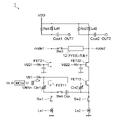
図1は、出力ポート間のアイソレーションを改善するアイソレーション改善回路を備える高周波増幅回路(以下、LNAと記載する)の回路図である。図1のLNA1は、例えば、SOI基板上に配置可能である。また、LNA1の周辺回路、例えば、アンテナスイッチとLNA1を同一のSOI基板上に配置してもよい。図1のLNA1は、例えば、携帯電話やスマートフォン等の無線装置で用いられるが、用途や実装場所は問わない。
FIG. 1 is a circuit diagram of a high frequency amplifier circuit (hereinafter referred to as LNA) including an isolation improving circuit for improving isolation between output ports. The
LNA1は、入力ポートLNAinと、2つの出力ポートである第1出力ポートOUT1と、第2出力ポートOUT2と、を備える。入力ポートLNAinから入力された信号を増幅し、いずれかの出力ポートから出力する単一出力モードと、双方の出力ポートから出力するスプリット出力モードとを備える。特に、単一出力モードは、第1出力ポートOUT1から信号を出力する第1単一出力モードと、第2出力ポートOUT2から信号を出力する第2単一出力モードと、を備える。以下においては、入力ポートLNAinをポート1、第1出力ポートOUT1をポート2、第2出力ポートOUT2をポート3とも記載し、ポート間のアイソレーションは、このポート番号に基づいて指定される。
The LNA1 has an input port LNAin and two output ports, a first output port OUT1 and a second output port OUT2. It has a single output mode in which a signal input from the input port LNAin is amplified and output from one of the output ports, and a split output mode in which the signal is output from both output ports. In particular, the single output mode comprises a first single output mode in which signals are output from the first output port OUT1 and a second single output mode in which signals are output from the second output port OUT2. In the following, the input port LNAin is also referred to as
LNA1は、第1出力ポートOUT1を備える第1増幅回路2と、第2出力ポートOUT2を備える第2増幅回路3と、アイソレーション改善回路10と、を備える。第1増幅回路2は、第1トランジスタFET11と、第3トランジスタFET21と、第1ソースインダクタLs1と、第1スイッチSw1と、第1出力整合抵抗Rd1と、第1出力整合インダクタLd1と、第1出力整合キャパシタCout1と、を備える。
The LNA 1 includes a
入力ポートLNAinに入力された高周波信号は、第1トランジスタFET11のゲートに入力される。電源電圧VDDと第3トランジスタFET21のドレインとの間に接続される第1出力ポートOUT1からこの入力された高周波信号が増幅されて出力される。すなわち、第1ソースインダクタLs1と、第1トランジスタFET11と、第3トランジスタFET21と、出力整合のための第1出力整合抵抗Rd1と、第1出力整合インダクタLd1と、第1出力整合キャパシタCout1により信号が増幅され、さらに、整合されて出力される。この動作は、一般的なソース接地FETとゲート接地FETを接続させたカスコード接続増幅回路によるLNAと同等の動作であるので、詳しい説明は省略する。 A high-frequency signal input to the input port LNAin is input to the gate of the first transistor FET11. The input high-frequency signal is amplified and output from the first output port OUT1 connected between the power supply voltage VDD and the drain of the third transistor FET21. That is, a signal is generated by a first source inductor Ls1, a first transistor FET11, a third transistor FET21, a first output matching resistor Rd1 for output matching, a first output matching inductor Ld1, and a first output matching capacitor Cout1. is amplified, matched and output. Since this operation is equivalent to that of an LNA using a general cascode-connected amplifier circuit in which a source-grounded FET and a gate-grounded FET are connected, detailed description thereof will be omitted.
なお、各種出力整合用の回路素子は、一例として示したものであり、以下に説明する実施形態における本質的な点ではない。すなわち、出力整合用の回路素子は、別の構成であっても構わないし、第1増幅回路2の外側、広義では、LNA1の外側において備えられているものであってもよい。
The circuit elements for various output matching are shown as an example, and are not essential points in the embodiments described below. That is, the circuit element for output matching may have a different configuration, or may be provided outside the
同様に、第2増幅回路3は、第2トランジスタFET12と、第4トランジスタFET22と、第2ソースインダクタLs2と、第2出力整合抵抗Rd2と、第2出力整合インダクタLd2と、第2出力整合キャパシタCout2と、を備え、入力端子LNAinに入力された高周波信号を第2出力ポートOUT2から増幅して出力する。
Similarly, the
これらの増幅回路において、スプリット出力モードの場合には、第1スイッチSw1及び第2スイッチSw2がオンとなり、双方の増幅回路がソースインダクタと接続され、信号が増幅されて出力する動作を行う。一方で、単一出力モードの場合、例えば、第1増幅回路のみから増幅信号を出力する場合には、第1スイッチSw1をオンに、第2スイッチSw2をオフにする。この結果、第1増幅回路においては信号を増幅してポート2から出力するが、第2増幅回路においては信号の増幅自体の動作を行わない。ゲートが高周波的に接地される第3トランジスタFET21及び第4トランジスタFET22のゲートに印加されるバイアス電圧も同様に制御してもよい。このように、単一出力モードにおいては、スイッチ及びトランジスタを出力するポートに対応してオン/オフ状態を切り替えてもよい。それぞれのトランジスタ、及び、スイッチの状態は、後述の各実施形態において詳しく記載する。
In these amplifier circuits, in the split output mode, the first switch Sw1 and the second switch Sw2 are turned on, both amplifier circuits are connected to the source inductor, and the signal is amplified and output. On the other hand, in the case of the single output mode, for example, when outputting the amplified signal only from the first amplifier circuit, the first switch Sw1 is turned on and the second switch Sw2 is turned off. As a result, the first amplifier circuit amplifies the signal and outputs it from the
アイソレーション改善回路10は、ポート2と、ポート3との間のアイソレーションを改善する回路である。アイソレーション改善回路10は、第3スイッチSw3と、アドミタンス素子12と、を備える。以下においては、アイソレーション改善回路のことをS23改善回路とも記載する。アイソレーション改善回路10は、第3トランジスタFET21のドレインと、第4トランジスタFET22のドレインとを接続する。
The
より詳しくは、信号を増幅するトランジスタと、出力ポート(出力整合回路)との間にS23改善回路10がこれらのポート同士を接続するように備えられる。すなわち、図に示すように、S23改善回路10は、第3トランジスタFET21と第1出力ポートOUT1との間のノードn1、及び、第4トランジスタFET22と第2出力ポートOUT2との間のノードn2の間を接続する。
More specifically, an
第3スイッチSw3は、例えば、スプリット出力モードにおいてオンとなり、単一出力モードにおいてオフとなるように制御されるスイッチである。このように、第3スイッチSw3により、出力モードに基づいて、S23改善回路10の接続状態を遷移させる。
The third switch Sw3 is, for example, a switch that is controlled to be ON in the split output mode and OFF in the single output mode. Thus, the connection state of the
ここで、入力ノードLNAinを接地電位とし、かつ、出力整合キャパシタCout1、Cout2およびS23改善回路10を取り除いた回路を仮想回路Aとし、前記仮想回路Aにおけるノードn1を第1ポート、ノードn2を第2ポートとしたときのYパラメータのY21成分をY21(A)とする。また、アドミタンス素子12の一方の端子を第1ポートとし、他方の端子を第2ポートとしたときのYパラメータのY21成分をY21(B)とする。
Here, a circuit in which the input node LNAin is grounded and the output matching capacitors Cout1 and Cout2 and the
本実施形態においては、Y21(B)=-Y21(A)になるように設定される。すなわち、アドミタンス素子12は、スプリット出力モードにおいてノードn1とノードn2との間のアドミタンスを打ち消す。それによりLNA1のS23が改善する。単純には、アドミタンス素子12は、例えば、直列に接続された抵抗とキャパシタとを備える。
In this embodiment, it is set so that Y21(B)=-Y21(A). That is,
このようなS23改善回路10を備えることにより、スプリット出力モードにおいては、第1出力端子OUT1と第2出力端子OUT2の間のアイソレーションが改善される。
By providing such an
図2は、スプリット出力モード時にノイズを低減するノイズ指数改善回路を備えるLNAの回路図である。上述のLNA1と同様に、例えば、SOI基板上に配置可能である。
FIG. 2 is a circuit diagram of an LNA with a noise figure improvement circuit that reduces noise when in split output mode. Like the
図2におけるLNA1において、上述した第1増幅回路2及び第2増幅回路3の構成は同様である。一方で、アイソレーション改善回路の代わりに、ノイズ指数改善回路20を備える。ノイズ指数改善回路20は、第1増幅回路2及び第2増幅回路3において、他方の増幅回路からのノイズを抑制する回路である。以下においては、ΔNF改善回路とも記載する。ΔNF改善回路20は、第1トランジスタFET11と第1スイッチSw1との間のノードn3、及び、第2トランジスタFET12と第2スイッチSw2との間のノードn4とを接続する。
In the
ΔNFは、(スプリット出力時のNF)-(単一出力時のNF)として表される値であり、スプリット出力時と単一出力時とのモード間におけるノイズ指数の差を表す。ΔNF改善回路20は、スプリット出力の場合にオンされ、スプリット出力時における出力のノイズを単一出力時における出力のノイズレベルまで低く抑えようとする回路である。
ΔNF is a value expressed as (NF at split output)−(NF at single output) and represents the difference in noise figure between split output and single output modes. The .
ΔNF改善回路20は、第4スイッチSw4と、キャパシタCsxと、を備える。第4スイッチSw4は、単一出力モード時には、オフとなり、ΔNF改善回路は、それぞれの増幅回路と接続されない状態となる。一方で、スプリット出力モードの場合、第4スイッチSw4がオンとなり、第1トランジスタFET11のソースと、第2トランジスタFET12のソースとの間にキャパシタCsxが接続される。
The
キャパシタCsxの役割を説明するため、第2トランジスタFET12のチャネルで発生したノイズが第1トランジスタFET11のゲートに回り込む様子を説明する。第2トランジスタFET12のチャネルで発生した電流ノイズはノードn4にノイズ電圧を誘起する。そのノイズ電圧は第2トランジスタFET12のゲート・ソース間容量を介して第1トランジスタFET11のゲートに回り込む。一方、容量Csxと第1トランジスタFET11のゲート・ソース間容量を介しても第1トランジスタFET11のゲートに回り込む。よって、両者の伝達経路の位相差が180°になるように調整されていれば、第2トランジスタFET12のチャネルで発生したノイズが第1トランジスタFET11のゲートに回り込む込むことはない。同様に、第1トランジスタFET11のチャネルで発生したノイズが第2トランジスタFET12のゲートに回り込むことはない。 In order to explain the role of the capacitor Csx, how the noise generated in the channel of the second transistor FET12 enters the gate of the first transistor FET11 will be explained. Current noise generated in the channel of the second transistor FET12 induces a noise voltage at the node n4. The noise voltage goes around the gate of the first transistor FET11 via the gate-source capacitance of the second transistor FET12. On the other hand, it also enters the gate of the first transistor FET11 via the capacitance Csx and the capacitance between the gate and source of the first transistor FET11. Therefore, if the phase difference between the two transmission paths is adjusted to 180°, noise generated in the channel of the second transistor FET12 will not flow into the gate of the first transistor FET11. Similarly, noise generated in the channel of the first transistor FET11 does not flow into the gate of the second transistor FET12.
本実施形態ではそのようにキャパシタCsxが調整されている。具体的にはLNA1の増幅対象である周波数帯の中心付近でΔNFが最小となるように調整されている。 In this embodiment, the capacitor Csx is adjusted in such a manner. Specifically, it is adjusted so that ΔNF is minimized near the center of the frequency band to be amplified by LNA1.
例えば、図に示す破線は、各トランジスタにおけるソース・ゲート間の寄生容量である。第2トランジスタFET12でノイズが発生すると、第2トランジスタFET12の寄生容量を介して、第1トランジスタFET11及び第2トランジスタFET12のゲートへとノイズが伝達される。ΔNF改善回路20が無い場合、このノイズは、入力信号に加算されて第1トランジスタFET11のゲートへと印加される。
For example, the dashed line in the figure is the parasitic capacitance between the source and gate in each transistor. When noise occurs in the second transistor FET12, the noise is transmitted to the gates of the first transistor FET11 and the second transistor FET12 via the parasitic capacitance of the second transistor FET12. Without the
そこで、このノイズの位相を180°ずらして、第1トランジスタFET11のソース・ゲート間の寄生容量を介して第1トランジスタFET11のゲートにフィードバックする信号をΔNF改善回路20において生成し、ノイズを打ち消す。同様に、第1トランジスタFET11でノイズが発生した場合にも、ΔNF改善回路により第1トランジスタFET11及び第2トランジスタFET12のゲートに印加されるノイズを相殺する。
Therefore, the phase of this noise is shifted by 180°, and a signal fed back to the gate of the first transistor FET11 via the parasitic capacitance between the source and gate of the first transistor FET11 is generated in the
図3は、ΔNF改善回路20の別の配置例を示すものである。この図3に示すように、ΔNF改善回路は、第1スイッチSw1と第1ソースインダクタLs1の間のノードn5、及び、第2スイッチSw2と第2ソースインダクタLs2との間のノードn6を接続するように備えられてもよい。
FIG. 3 shows another arrangement example of the
なお、上記においては、増幅回路内の信号増幅のトランジスタを2段で構成するものとしたが、3段以上の構成であってもよい。例えば、第1増幅回路は、第1トランジスタFET11と、第3トランジスタFET21に加え、同じく高周波的にゲートが接地される第5トランジスタを備えてもよい。第5トランジスタは、そのソースが第3トランジスタFET21のドレインと接続するように直列に、第3トランジスタFET21とポート2との間に備えられる。
In the above description, the transistors for signal amplification in the amplifier circuit are configured in two stages, but may be configured in three or more stages. For example, in addition to the first transistor FET11 and the third transistor FET21, the first amplifier circuit may also include a fifth transistor whose gate is grounded at high frequencies. A fifth transistor is provided between the third transistor FET21 and
図4は、LNA1の具体的な実装例である。LNA1は、第1増幅回路2と、第2増幅回路3と、S23改善回路10と、ΔNF改善回路20と、に加え、例えば、SPnTスイッチ4と、入力整合回路5と、をさらに備える。
FIG. 4 is a specific implementation example of LNA1. In addition to the
SPnTスイッチ4(Single-Pole n-Throw Switch)は、n個のバンドに対応したn個の入力信号INの中から増幅すべき信号を選択するバンドセレクトスイッチである。例えば、Band7(2620MHz~2690MHz)とBand41(2496MHz~2690MHz)のどちらかを選択して増幅する場合、Band7はBand41に包含されるため、Band41用に設計された増幅回路の前段にSPDT (Single-Pole Double-Throw)スイッチが設けられる。
The SPnT switch 4 (Single-Pole n-Throw Switch) is a band select switch that selects a signal to be amplified from n input signals IN corresponding to n bands. For example, when selecting and amplifying either Band 7 (2620 MHz to 2690 MHz) or Band 41 (2496 MHz to 2690 MHz),
以下で説明するLNA1には、Band41の周波数帯に属する周波数の信号を選択して出力する。第1増幅回路2及び第2増幅回路3以外にも、多数の周波数帯に対応する増幅回路を、LNA1は、備えていてもよいし、SPnTスイッチ4からLNA1の外部の増幅回路に対して出力をしてもよい。この場合複数のLNA等をSPnTスイッチ4と同一のSOI基板上に備えてもよい。
A signal of a frequency belonging to the frequency band of Band 41 is selected and output to
SPnTスイッチ4から出力された信号は、端子SWoutからいったん外部へと出力され、外部インダクタLextを介して入力信号として、入力ポートLNAinから入力される。外部インダクタLextと並列に、LNA1内に、入力整合回路5を備えてもよい。
The signal output from the
入力された信号は、上述のように、並列に備えられた第1増幅回路2及び第2増幅回路3において増幅され、単一出力又はスプリット出力のモードにより出力される。出力ポート間のアイソレーション特性又はノイズ特性は、これら2つの増幅回路の間に少なくともいずれか1つが備えられたS23改善回路10及びΔNF改善回路20を介して改善される。
An input signal is amplified by the
なお、図4には示されていないが、各ブロックは、必要に応じて、電源電圧Vdd、Vss(又はGND)と接続され、必要な電力が供給される。また、回路中の各トランジスタには、必要に応じて(例えば、出力モードに応じて)そのゲートにバイアス電圧が外部から印加される。LNA1は、これらの電源電圧、バイアス電圧等の入力を受け付ける入力端子が備えられていてもよい。また、ゲートにバイアス電圧を印加する場合には、高周波雑音を抑制する抵抗と接地キャパシタ等を必要に応じて備えてもよい。
Although not shown in FIG. 4, each block is connected to power supply voltages Vdd and Vss (or GND) as necessary to supply necessary power. A bias voltage is externally applied to the gate of each transistor in the circuit as required (for example, depending on the output mode). The
以下、これらの回路について、より具体的な実施形態を示し、説明する。 More specific embodiments of these circuits will be shown and described below.
(第1実施形態)
図5は、本実施形態に係るLNA1の一例を示す図である。以下の実施形態においては、一例としてBand41の周波数帯(2496MHz-2690MHz)について説明するが、これに限られるものではない。例えば、他の周波数帯に対しては、回路定数を変えた回路素子を用いることにより同様の回路構成により性能を向上させる。
(First embodiment)
FIG. 5 is a diagram showing an example of the
第1増幅回路2及び第2増幅回路3は、基本的には、前述したものと同様である。第1増幅回路2は、さらに、第1単一出力モードにおいてオンする第5スイッチFETsw5aと、第5スイッチFETsw5aにより接続状態が制御されるキャパシタCin1が備えられる。同様に、第2増幅回路3は、第6スイッチFETsw5bと、キャパシタCin2が備えられる。これらのキャパシタは、入力側における整合回路として動作する。すなわち、これらのキャパシタは、単一出力モードは、スプリット出力モードと比較してインピーダンスが変化するため、両出力モードにおけるインピーダンスを整合するために備えられる。
The
第1出力整合抵抗Rd1、第2出力整合抵抗Rd2は、利得調整を行うべく図に示すように可変抵抗としてもよい。さらに、各出力モードに対応して出力ポートから信号を出力するか否かを決定する第1出力スイッチSW1、第2出力スイッチSW2が備えていてもよい。すなわち、第1単一出力モード及びスプリット出力モードにおいてオンされ、第2出力モードにおいてオフされる第1出力スイッチSW1と、第2単一出力モード及びスプリット出力モードにおいてオンされ、第1出力モードにおいてオフされる第2出力スイッチSW2を備えていてもよい。 The first output matching resistor Rd1 and the second output matching resistor Rd2 may be variable resistors as shown in the figure for gain adjustment. Furthermore, a first output switch SW1 and a second output switch SW2 for determining whether or not to output a signal from the output port corresponding to each output mode may be provided. That is, a first output switch SW1 that is turned on in the first single output mode and the split output mode and turned off in the second output mode, and a first output switch SW1 that is turned on in the second single output mode and the split output mode and is turned on in the first output mode. A second output switch SW2 that is turned off may be provided.
LNA1は、第1増幅回路2と第2増幅回路3とを接続するS23改善回路10と、ΔNF改善回路20と、を備える。
The
S23改善回路10は、それぞれの増幅回路側において、第3スイッチFETsw3a、FETsw3bを備える。これらのスイッチの間に、アドミタンス素子12として直列に接続された抵抗Rdxと、キャパシタCdxを備える。抵抗Rdx及びキャパシタCdxは、前述したように、ノードn1とノードn2との間におけるアドミタンスを打ち消す値を有するように調整される。
The
第3スイッチFETsw3a、FETsw3bは、ゲート同士が接続されていてもよい。これらのスイッチは、スプリット出力モードにおいてオンされ、第1単一出力モード及び第2単一出力モードにおいてオフされるようにゲートに信号が入力される。例えば、第3スイッチFETsw3a、FETsw3bは、p型のMOSFETを備える。 Gates of the third switches FETsw3a and FETsw3b may be connected to each other. These switches are signaled to the gates so that they are turned on in the split output mode and turned off in the first single output mode and the second single output mode. For example, the third switches FETsw3a and FETsw3b are provided with p-type MOSFETs.
ΔNF改善回路20は、ノードn3、n4の間に接続され、それぞれの増幅回路側において、第4スイッチFETsw4a、FETsw4bを備える。これらのスイッチの間に、ΔNF改善キャパシタCsx(ノイズ指数改善素子)が備えられる。ΔNF改善キャパシタCsxは、前述したように、第2トランジスタFET12から第1トランジスタFET11へと伝達するノイズが、周波数帯の中央付近、例えば、Band41の周波数帯の中央付近において位相が180°ずれる(反転する)ようにその値が調整される。
The
第4スイッチFETsw4a、FETsw4b(ノイズ指数改善回路第1/第2切替スイッチ)は、ゲート同士が接続されていてもよい。これらのスイッチは、スプリット出力モードにおいてオンされ、第1単一出力モード及び第2単一出力モードにおいてオフされるようにゲートに信号が入力される。例えば、第4スイッチFETsw4a、FETsw4bは、n型のMOSFETを備える。 Gates of the fourth switches FETsw4a and FETsw4b (noise figure improvement circuit first/second selector switch) may be connected to each other. These switches are signaled to the gates so that they are turned on in the split output mode and turned off in the first single output mode and the second single output mode. For example, the fourth switches FETsw4a and FETsw4b comprise n-type MOSFETs.
LNA1は、さらに、第1増幅回路2のノードn5、及び、第2増幅回路3のノードn6と入力ポートLNAinとの間にそれぞれ接続された、静電気放電保護回路(以下、ESD保護回路と記載する)D1、D2を備える。ESD保護回路D1、D2は、入力側のESDから増幅回路の保護を行う回路である。ESD保護回路D1、D2は、例えば、PN接合ダイオードを図に示すように、並列に逆向きに配置して構成される。従来のESD保護回路は入力ポートLNAinと接地電位との間に設けられるが、図5のように接続することで、ESD保護回路D1の寄生容量が第1増幅回路の入力整合回路の一部となり、ESD保護回路D2の寄生容量が第2増幅回路の入力整合回路の一部となるため、入力反射特性が改善する。
The
図6は、図5の回路において、各モードにおけるスイッチの状態又は印加される電圧の状態を示す表である。出力モードは、単一出力モード及びスプリット出力モードのことを示す。アクティブ出力とは、信号が出力されるポートを示す。第1単一出力モードでは、出力ポートOUT1が、第2単一出力モードでは、出力ポートOUT2が、スプリット出力モードでは、出力ポートOUT1、OUT2がアクティブ出力となる。 FIG. 6 is a table showing the state of the switch or the state of the applied voltage in each mode in the circuit of FIG. Output mode refers to single output mode and split output mode. An active output indicates a port from which a signal is output. In the first single output mode, the output port OUT1 is the active output, in the second single output mode the output port OUT2 is the active output, and in the split output mode the output ports OUT1 and OUT2 are the active outputs.
VB21、VB22は、それぞれ、第3トランジスタFET21のゲート、第4トランジスタFET22のゲートへ印加されるバイアス電圧である。Cont1、Cont2、Cont3及びCont4は、それぞれ、第1単一出力モードを動作させる信号、第2単一出力モードを動作させる信号、いずれかの単一出力モードを動作させる信号及びスプリット出力モードを動作させる信号である。 VB21 and VB22 are bias voltages applied to the gate of the third transistor FET21 and the gate of the fourth transistor FET22, respectively. Cont1, Cont2, Cont3 and Cont4 are respectively the signal to operate the first single output mode, the signal to operate the second single output mode, the signal to operate any single output mode and the split output mode. It is a signal to let
第1出力整合抵抗Rd1、第2出力整合抵抗Rd2は、各出力ポートから出力される信号の利得を調整するために、可変抵抗としている。その抵抗値を示すのがRd1、Rd2の列で示される。SW1、SW2は、それぞれ第1出力スイッチSW1及び第2出力スイッチSW2のオン/オフ状態を示す。 The first output matching resistor Rd1 and the second output matching resistor Rd2 are variable resistors for adjusting the gain of the signal output from each output port. Columns Rd1 and Rd2 show the resistance values. SW1 and SW2 indicate the ON/OFF states of the first output switch SW1 and the second output switch SW2, respectively.
図6に示すように各スイッチ等に信号が入力されると、図5におけるLNA1において、第1単一出力モード、第2単一出力モード、及び、スプリット出力モードのモードが変更される。
When a signal is input to each switch or the like as shown in FIG. 6, the mode of the first single output mode, the second single output mode, and the split output mode is changed in the
例えば、図6に示すように第1単一出力モード、すなわち、出力モードが単一出力でアクティブ出力がOUT1である場合、VB21がオンされることにより、第3トランジスタFET21がオンに、Cont1をHighとすることにより、第1スイッチFETsw1がオンに、Cont3をHighとすることにより、第5スイッチFETsw5aがオンに、そして、SW1がオンになる。 For example, as shown in FIG. 6, in the first single output mode, i.e., when the output mode is single output and the active output is OUT1, VB21 is turned on, thereby turning on the third transistor FET21 and turning Cont1 on. By setting Cont3 to High, the first switch FETsw1 is turned on, and by setting Cont3 to High, the fifth switch FETsw5a is turned on, and SW1 is turned on.
この場合、入力された信号は、キャパシタCxを介して第1トランジスタFET11のゲートにバイアス電圧VB1でバイアスを掛けられて入力され、かつ、第1トランジスタFET11は、第1スイッチFETsw1がオンすることにより第1ソースインダクタLs1を介して接地される。キャパシタCx及び第1ソースインダクタは、入力整合回路として機能する。また、キャパシタCxには、信号の直流成分を除去する機能もある。そして、第5スイッチFETsw5aがオンになることにより、ゲート-ソース間にキャパシタが接続される。第1トランジスタFET11のドレインは、第3トランジスタFET21のソースと接続され、第1出力整合回路を介して第1出力ポートOUT1から出力される。 In this case, the input signal is biased by the bias voltage VB1 to the gate of the first transistor FET11 through the capacitor Cx, and the first transistor FET11 is turned on by turning on the first switch FETsw1. It is grounded through the first source inductor Ls1. Capacitor Cx and the first source inductor function as an input matching circuit. Capacitor Cx also has the function of removing the DC component of the signal. A capacitor is connected between the gate and the source by turning on the fifth switch FETsw5a. The drain of the first transistor FET11 is connected to the source of the third transistor FET21, and output from the first output port OUT1 via the first output matching circuit.
一方で、バイアス電圧VB22がオフされることにより、第2増幅回路の第4トランジスタFET22は、オフとなる。同様に、Cont2をLowとすることにより、第2スイッチFETsw2がオフとなる。Cont3をHighとすることにより、S23改善回路10は、第3スイッチFETsw3a、FETsw3bがオフとなり、動作しない。同様に、Cont4をLowとすることにより、ΔNF改善回路20も、動作しない。このように、出力ポートOUT1から増幅された信号が出力されることとなる。
On the other hand, turning off the bias voltage VB22 turns off the fourth transistor FET22 of the second amplifier circuit. Similarly, setting Cont2 to Low turns off the second switch FETsw2. By setting Cont3 to High, the
この場合、第1出力整合抵抗Rd1を小さくすることにより、単一出力モードの利得が抑えられ、スプリット出力モードとの利得差が抑えられる。第2増幅回路3のみから出力する第2単一出力モードについても、同様の動作を行う。
In this case, by reducing the first output matching resistor Rd1, the gain in the single output mode is suppressed, and the gain difference with the split output mode is suppressed. The same operation is performed in the second single output mode in which only the
スプリット出力モードである場合、VB21、VB22をともにオン、Cont1、Cont2をともにHighとし、SW1、SW2をともにオンとすることから、第3トランジスタFET21、第4トランジスタFET22、第1スイッチFETsw1、第2スイッチFETsw2が全てオンとなる。このため、第1増幅回路2、第2増幅回路3ともに出力ポートと接続され、各出力ポートから信号が出力される。
In the split output mode, both VB21 and VB22 are turned on, Cont1 and Cont2 are both set to High, and both SW1 and SW2 are turned on. All switches FETsw2 are turned on. Therefore, both the
さらに、Cont3をLowとすることから、キャパシタCin1、Cin2が動作しない状態となり、かつ、第3スイッチFETsw3a、FETsw3bがともにオンとなりS23改善回路10がノードn1、n2間において、第1増幅回路2と第2増幅回路3とを接続する。また、Cont4をHighとすることから、第4スイッチFETsw4a、FETSw4bがともにオンとなり、ΔNF改善回路20がノードn3、n4間において第1増幅回路2と第2増幅回路3とを接続する。
Furthermore, since Cont3 is set to Low, the capacitors Cin1 and Cin2 do not operate, and both the third switches FETsw3a and FETsw3b are turned on, so that the
このように、図6のように制御信号を入力することにより、各単一出力モード及びスプリット出力モードの3つの出力モードを切り替えることが可能となる。さらに、スプリット出力モードにおいては、S23改善回路10と、ΔNF改善回路20の双方の回路がアクティブな状態となる。
Thus, by inputting the control signal as shown in FIG. 6, it is possible to switch between the three output modes of each single output mode and split output mode. Furthermore, in the split output mode, both the
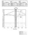
以下、本実施形態の単一出力モード時及びスプリット出力モード時における入出力特性を示すパラメータ等についてシミュレーション結果を記載する。例えば、電源電圧を1.8Vとし、対象とする周波数帯域をBand41とした。以下の図面において、Sパラメータのグラフについては、m1は、周波数2496MHzにおける観測、m2は、周波数2593MHzにおける観測、m3は、周波数2690MHzにおける観測を示す。また、NFのグラフについては、m4は、周波数2496MHzにおける観測、m5は、周波数2593MHzにおける観測、m6は、周波数2690MHzにおける観測を示す。 Simulation results will be described below for parameters and the like indicating the input/output characteristics in the single output mode and the split output mode of this embodiment. For example, the power supply voltage is set to 1.8V, and the target frequency band is set to Band41. In the following figures, for the S-parameter graphs, m1 indicates observations at a frequency of 2496 MHz, m2 indicates an observation at a frequency of 2593 MHz, and m3 indicates an observation at a frequency of 2690 MHz. In the NF graph, m4 indicates observation at a frequency of 2496 MHz, m5 indicates observation at a frequency of 2593 MHz, and m6 indicates observation at a frequency of 2690 MHz.
図7は、本実施形態に係るLNA1による単一出力モード時の入出力特性であるSパラメータ(Scattering Parameter)を示す図である。記述の簡単のために、入力ポートをポート1、出力ポートをポート2又はポート3として各Sパラメータを、S21等と表す。実線は、S21を、破線は、S11を、点線は、S22を示す。
FIG. 7 is a diagram showing the S parameter (Scattering Parameter), which is the input/output characteristic of the
入力信号に対する出力信号の増幅の度合いはS21で表すことができる。S21は、着目している周波数帯域(Band41)において大きいほど利得が高いことを示す。入力信号に対し、入力側のポートに対する反射の度合い(反射特性)は、S11で表され、高周波回路においては、入出力ポートにおいて原則的にインピーダンス整合が求められるので、低いこと(例えば、-10dB以下であること)が望まれる。 The degree of amplification of the output signal with respect to the input signal can be represented by S21. S21 indicates that the higher the gain in the frequency band of interest (Band41), the higher the gain. The degree of reflection (reflection characteristic) of the input signal to the port on the input side is represented by S11. In a high-frequency circuit, impedance matching is required in principle at the input/output port, so it should be low (eg, -10 dB below) is desired.
図に示すように、S21のカーブは、着目している周波数帯域において高い値であることが分かる。一方で、S11及びS22のカーブは、着目している周波数帯域において低く抑えられていることが分かる。 As shown in the figure, it can be seen that the curve of S21 has a high value in the frequency band of interest. On the other hand, it can be seen that the curves of S11 and S22 are kept low in the frequency band of interest.
図の上部に示している数値は、各観測点における各パラメータの数値を表す。単一出力モードにおける利得は、18dBである。また、S11は、一般的に帯域内において要求される値(-8dB以下)を満たしている。S22も、一般的に帯域内において要求される値(-12dB以下)を満たしている。 The numerical values shown in the upper part of the figure represent the numerical values of each parameter at each observation point. The gain in single output mode is 18 dB. Also, S11 generally satisfies the value (-8 dB or less) required within the band. S22 also generally satisfies the value (-12 dB or less) required within the band.
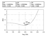
図8は、本実施形態に係るLNA1による単一出力モード時のノイズ指数(NF:Noise Figure)を示す図である。観測した周波数帯において、NFは、0.86dBを超えない程度のよい特性を示している。
FIG. 8 is a diagram showing the noise figure (NF) in the single output mode of the
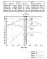
図9は、本実施形態に係るLNA1によるスプリット出力モード時のSパラメータを示す図である。一点鎖線は、S23を示す。入力信号に対する出力信号の増幅の度合いは、上述したように、S21で表される。上述した単一出力モードと同様に、入力ポートに対する反射は、S11、出力ポートに対する反射はS22とする。さらに、スプリット出力モード固有の問題として、出力ポート間の信号の伝播が問題となる。このポート3からポート2への伝達特性を示すSパラメータをS23として表す。なお、S31、S32、S33に関しては示していないが、第1増幅回路2と第2増幅回路3の回路定数を同じとしているため、基本的にはS21、S23、S22と同様の結果を得ることができる。
FIG. 9 is a diagram showing S-parameters in the split output mode of the
図に示すように、S21のカーブは、着目している周波数帯域において高い値であることが分かる。一方で、S11、S22及びS23のカーブは、着目している周波数帯域において低く抑えられていることが分かる。スプリット出力モードの利得は、17dBである。また、S23は、-35.1dB以下であり、一般的に要求される値(-25dB以下)を満たしている。 As shown in the figure, it can be seen that the curve of S21 has a high value in the frequency band of interest. On the other hand, it can be seen that the curves of S11, S22 and S23 are kept low in the frequency band of interest. The gain in split output mode is 17 dB. Also, S23 is -35.1 dB or less, which satisfies a generally required value (-25 dB or less).
単一出力モードにおけるS23は、明示していないが、SW1、SW2のうち、オフ状態のアイソレーションにより、ポート2、ポート3間のアイソレーションが確保される。
Although S23 in the single output mode is not shown, isolation between
図10は、本実施形態に係るLNA1によるスプリット出力モード時のノイズ指数を示す図である。観測した周波数帯において、1.03dBを超えない程度のよい特性を示している。また、スプリット出力モードにおける帯域中心のノイズ指数が、単一出力モードに対して、0.11dBしか劣化していないことに留意されたい。
FIG. 10 is a diagram showing the noise figure in the split output mode of the
図11は、上記説明したパラメータ等をまとめたものである。Idd_lnaは、LNA1に入力されるバイアス電流のことを示す。バイアス電流Idd_lnaは、高周波信号が入力されていない場合に、VDD端子からLNA1へと流れ込む電流である。一般に、バイアス電流を適切な範囲で大きい値に設定すると、高い利得を得ることができる。本実施形態においては、一例として、単一出力モードでは、6.3mA、スプリット出力モードでは、12.6mAとしている。 FIG. 11 summarizes the parameters and the like described above. Idd_lna indicates the bias current input to LNA1. The bias current Idd_lna is a current that flows from the VDD terminal to the LNA1 when no high-frequency signal is input. In general, a high gain can be obtained by setting the bias current to a large value within an appropriate range. In this embodiment, as an example, it is 6.3 mA in the single output mode and 12.6 mA in the split output mode.
fcenterは、帯域の中央の周波数、すなわち、図中におけるm2、m5における結果を示す。帯域内と示された箇所は、帯域内で最も悪い結果を記載したものである。 fcenter indicates the center frequency of the band, that is, the results at m2 and m5 in the figure. The places labeled in-band describe the worst in-band results.
S23改善回路10と、ΔNF改善回路20の効果について、比較例を示して記載する。下記の例においては、それぞれスプリット出力モードにおける結果を示している。
The effects of the
図12は、S23改善回路10が無い場合のLNAと、本実施形態に係るLNA1について、ポート2とポート3との間の伝達特性を示すグラフである。ターゲットである周波数帯において、本実施形態に係るLNA1は、十分に小さいS23の値を有していることがわかる。上述したように、これらは、一般的に要求される値より十分小さい値を取っている。
FIG. 12 is a graph showing transfer characteristics between
一方で、S23改善回路10が無い場合のLNAは、比較例Aとして破線で示されている。グラフから分かるように、本実施形態に比べて大きい値を取っていることが分かる。さらには、一般的に要求される値-25dBを大きく上回る結果となっている。このことから、S23改善回路10は、出力間アイソレーションを改善する効果を奏していることが分かる。
On the other hand, the LNA without the
図13は、ΔNF改善回路20が無い場合のLNAと、本実施形態に係るLNA1について、NFを示すグラフである。ターゲットである周波数帯において、本実施形態に係るLNA1は、十分に小さいNFの値を有していることが分かる。上述したように、よいノイズ特性を有している。
FIG. 13 is a graph showing NF for the LNA without the
一方で、ΔNF改善回路20が無い場合のLNAは、比較例Bとして破線で示されている。グラフから分かるように、本実施形態に比べて大きい値を取っていることが分かる。このことから、ΔNF改善回路20は、ノイズ指数を改善する効果を奏していることが分かる。
On the other hand, the LNA without the
以上のように、本実施形態によれば、単一出力モードとスプリット出力モードを有するLNAについて、出力間アイソレーションを改善するS23改善回路10と、ノイズ特性を改善するΔNF改善回路20と、を備えることにより、出力間アイソレーションを高めるとともに、ノイズを低減させることが可能である。また、バンドセレクトスイッチとして機能するSPnTスイッチ4と同じSOI上に各増幅回路等を配置できるため、小型化及び低消費電力化も望むことができる。さらに、ESD保護回路を有することにより、静電気放電についても耐性を有する。
As described above, according to the present embodiment, for an LNA having a single output mode and a split output mode, the
(第2実施形態)
図14は、本実施形態に係るLNA1の一例を示す図である。第1増幅回路2及び第2増幅回路3は、基本的に前述の第1実施形態と同様である。S23改善回路10及びΔNF改善回路20についても、前述の第1実施形態と同様であるが、ΔNF改善回路20は、ノードn5、n6間において第1増幅回路2と第2増幅回路3とを接続する。
(Second embodiment)
FIG. 14 is a diagram showing an example of the
また、LNA1内において直列に接続された入力整合キャパシタC1と第7スイッチFETsw6を備える入力整合回路5が外部インダクタLextと並行に接続される。この入力整合回路5は、前述した図5における第5スイッチFETsw5aとキャパシタCin1及び第6スイッチFETsw5bとキャパシタCin2の代わりに備えられる。単一出力モードにおいてキャパシタC1がオンし、スプリット出力モードにおいてキャパシタC1がオフするようにスイッチされる。
An
図14の回路において、各モードのスイッチ状態又は印加される電圧の状態は、第1実施形態と同様に図6に示す通りである。Cont3がHigh、すなわち、単一出力モードの場合には、第7スイッチFETsw6がオンとなり、キャパシタC1が外部インダクタLextと並列に接続され、入力信号の整合を行う。図6に示すように各スイッチ等に信号が入力されると、図14におけるLNA1において、第1単一出力モード、第2単一出力モード、及び、スプリット出力モードのモードが変更される。 In the circuit of FIG. 14, the switching state of each mode or the state of applied voltage is as shown in FIG. 6, as in the first embodiment. When Cont3 is High, ie in single output mode, the seventh switch FETsw6 is turned on and the capacitor C1 is connected in parallel with the external inductor Lext to match the input signal. When a signal is input to each switch or the like as shown in FIG. 6, the mode of the first single output mode, second single output mode, and split output mode is changed in LNA1 in FIG.
以下、本実施形態の単一出力モード時及びスプリット出力モード時における入出力特性を示すパラメータ等についてシミュレーション結果を記載する。例えば、電源電圧を1.8Vとし、対象とする周波数帯域をBand41とした。 Simulation results will be described below for parameters and the like indicating the input/output characteristics in the single output mode and the split output mode of this embodiment. For example, the power supply voltage is set to 1.8V, and the target frequency band is set to Band41.
図15は、本実施形態に係るLNA1による単一出力モード時の入出力特性であるSパラメータを示す図である。
FIG. 15 is a diagram showing S parameters, which are the input/output characteristics of the
図に示すように、S21のカーブは、着目している周波数帯域において高い値であることが分かる。一方で、S11及びS22のカーブは、着目している周波数帯域において低く抑えられていることが分かる。 As shown in the figure, it can be seen that the curve of S21 has a high value in the frequency band of interest. On the other hand, it can be seen that the curves of S11 and S22 are kept low in the frequency band of interest.
単一出力モードにおける利得は、18dB程度である。また、S11は、一般的に帯域内において要求される値(-8dB以下)を満たしている。S22も、一般的に帯域内において要求される値(-12dB以下)を満たしている。 The gain in single output mode is on the order of 18 dB. Also, S11 generally satisfies the value (-8 dB or less) required within the band. S22 also generally satisfies the value (-12 dB or less) required within the band.
図16は、本実施形態に係るLNA1による単一出力モード時のノイズ指数を示す図である。観測した周波数帯において、NFは、0.77dBを超えない程度のよい特性を示している。
FIG. 16 is a diagram showing the noise figure in the single output mode of the
図17は、本実施形態に係るLNA1によるスプリット出力モード時のSパラメータを示す図である。S21のカーブは、着目している周波数帯域において高い値であることが分かる。一方で、S11、S22及びS23のカーブは、着目している周波数帯域において低く抑えられていることが分かる。スプリット出力モードの利得は、17dB程度である。また、S23は、-32.4dB以下であり、一般的に要求される値(-25dB以下)を満たしている。
FIG. 17 is a diagram showing S-parameters in the split output mode of the
単一出力モードにおけるS23は、明示していないが、SW1、SW2のうち、オフ状態のアイソレーションにより、ポート2、ポート3間のアイソレーションが確保される。
Although S23 in the single output mode is not shown, isolation between
図18は、本実施形態に係るLNA1によるスプリット出力モード時のノイズ指数を示す図である。観測した周波数帯において、0.85dBを超えない程度のよい特性を示している。また、スプリット出力モードにおける帯域中心のノイズの指数が、単一出力モードに対して、0.076dBしか劣化していないことに留意されたい。
FIG. 18 is a diagram showing the noise figure in the split output mode of the
図19は、上記説明したパラメータ等をまとめたものである。本実施形態においては、バイアス電流を、一例として、単一出力モードでは、6.3mA、スプリット出力モードでは、12.6mAとしている。 FIG. 19 summarizes the parameters and the like described above. In this embodiment, for example, the bias current is 6.3 mA in the single output mode and 12.6 mA in the split output mode.
以上のように、本実施形態によっても、単一出力モードとスプリット出力モードを有するLNAについて、出力間アイソレーションを改善するS23改善回路10と、ノイズ特性を改善するΔNF改善回路20と、を備えることにより、出力間アイソレーションを高めるとともに、ノイズを低減させることが可能である。同様に、バンドセレクトスイッチとして機能するSPnTスイッチ4と同じSOI上に各増幅回路等を配置できるため、小型化及び低消費電力化も望むことができる。
As described above, according to the present embodiment, an LNA having a single output mode and a split output mode is provided with the
図20は、本実施形態において、ΔNF改善回路20の接続箇所をノードn3、n4との間にしたものである。すなわち、図2の位置にΔNF改善回路20を移動したものである。このように接続位置をかえることによっても、同様の効果を得ることが可能である。
FIG. 20 shows that the
(第3実施形態)
図21は、本実施形態に係るLNA1の一例を示す図である。第1増幅回路2及び第2増幅回路3は、基本的に第1実施形態と同様であるが、ゲート接地するトランジスタを1段増やしたものである。また、これらのゲート接地のトランジスタを増やす代わりに、S23改善回路10を削除したものである。
(Third embodiment)
FIG. 21 is a diagram showing an example of the
第1増幅回路2は、高周波的にゲート接地する第3トランジスタFET21のドレインと第1出力整合回路との間に、さらに、第5トランジスタFET31を備える。第5トランジスタFET31は、ゲートが高周波的に接地され、ソースが第3トランジスタFET21のドレインと接続され、ドレインが第1出力整合回路を介して出力ポートOUT1と接続される。
The
同様に、第2増幅回路3は、高周波的にゲート接地する第6トランジスタFET32を備え、第6トランジスタFET32は、そのソースが第4トランジスタFET22のドレインと接続され、ドレインが第2出力整合回路を介して出力ポートOUT2と接続される。
Similarly, the
これらの第5トランジスタFET31及び第6トランジスタFET32には、第3トランジスタFET21及び第4トランジスタFET22とそれぞれ同期して同じオン・オフ状態となるようなバイアス電圧が印加される。 A bias voltage is applied to the fifth transistor FET31 and the sixth transistor FET32 such that they are in the same ON/OFF state in synchronization with the third transistor FET21 and the fourth transistor FET22, respectively.
なお、各出力整合回路に別々の電源電圧VDD1、VDD2が入力されているが、これには限られない。例えば、前述のLNA1と同様に、VDD1、VDD2は、共通のVDDであってもよい。 Although separate power supply voltages VDD1 and VDD2 are input to each output matching circuit, the present invention is not limited to this. For example, similar to LNA1 described above, VDD1 and VDD2 may be a common VDD.
図22は、各モードのスイッチの状態又は印加させる電圧の状態を示す表である。基本的には、前述の第1実施形態及び第2実施形態と同様であるが、第5トランジスタFET31及び第6トランジスタFET32のゲートに印加する電圧が追記されている。この表に示すように、第3トランジスタFET21のゲートに印加されるバイアス電圧VB21と第5トランジスタFET31のゲートに印加されるバイアス電圧VB31は、各モードにおいて同様の制御がされる。 FIG. 22 is a table showing the state of the switches in each mode or the state of the voltage to be applied. Although it is basically the same as the first and second embodiments described above, voltages applied to the gates of the fifth transistor FET31 and the sixth transistor FET32 are added. As shown in this table, the bias voltage VB21 applied to the gate of the third transistor FET21 and the bias voltage VB31 applied to the gate of the fifth transistor FET31 are similarly controlled in each mode.
すなわち、第1単一出力モード及びスプリット出力モードにおいては、これらのバイアス電圧VB21、VB31は、オンとなり、第2単一出力モードにおいては、オフとなる。このように制御されることにより、第1増幅回路2からの出力を制御する。第6トランジスタFET32のゲートに印加されるバイアス電圧VB32も同様であり、第2増幅回路3からの出力がある第2単一出力モード及びスプリット出力モードにおいては、オンとなり、第1単一出力モードにおいては、オフとなる。なお、VB31とVB32のオン時の電圧はVB21とVB22のオン時の電圧よりも高いことが望ましい。
That is, these bias voltages VB21 and VB31 are on in the first single output mode and the split output mode, and off in the second single output mode. By being controlled in this manner, the output from the
以下、本実施形態の単一出力モード時及びスプリット出力モード時における入出力特性を示すパラメータ等についてシミュレーション結果を記載する。例えば、電源電圧を1.8Vとし、対象とする周波数帯域をBand41とした。 Simulation results will be described below for parameters and the like indicating the input/output characteristics in the single output mode and the split output mode of this embodiment. For example, the power supply voltage is set to 1.8V, and the target frequency band is set to Band41.
図23は、本実施形態に係るLNA1による単一出力モード時の入出力特性であるSパラメータを示す図である。
FIG. 23 is a diagram showing S parameters, which are the input/output characteristics of the
図に示すように、S21のカーブは、着目している周波数帯域において高い値であることが分かる。一方で、S11及びS22のカーブは、着目している周波数帯域において低く抑えられていることが分かる。 As shown in the figure, it can be seen that the curve of S21 has a high value in the frequency band of interest. On the other hand, it can be seen that the curves of S11 and S22 are kept low in the frequency band of interest.
単一出力モードにおける利得は、18dB程度である。また、S11は、一般的に帯域内において要求される値(-8dB以下)を満たしている。S22も、一般的に帯域内において要求される値(-12dB以下)を満たしている。 The gain in single output mode is on the order of 18 dB. Also, S11 generally satisfies the value (-8 dB or less) required within the band. S22 also generally satisfies the value (-12 dB or less) required within the band.
図24は、本実施形態に係るLNA1による単一出力モード時のNFを示す図である。観測した周波数帯において、NFは、0.89dBを超えない程度のよい特性を示している。
FIG. 24 is a diagram showing NF in single output mode by
図25は、本実施形態に係るLNA1によるスプリット出力モード時のSパラメータを示す図である。S21のカーブは、着目している周波数帯域において高い値であることが分かる。一方で、S11、S22及びS23のカーブは、着目している周波数帯域において低く抑えられていることが分かる。スプリット出力モードの利得は、17dB程度である。また、S23は、-30.2dB以下であり、一般的に要求される値(-25dB以下)を満たしている。
FIG. 25 is a diagram showing S-parameters in the split output mode by the
単一出力モードにおけるS23は、明示していないが、SW1、SW2のうち、オフ状態のアイソレーションにより、ポート2、ポート3間のアイソレーションが確保される。
Although S23 in the single output mode is not shown, isolation between
図26は、本実施形態に係るLNA1によるスプリット出力モード時のノイズ指数を示す図である。観測した周波数帯において、0.94dBを超えない程度のよい特性を示している。また、スプリット出力モードにおける帯域中心のノイズ指数が、単一出力モードに対して、0.04dBしか劣化していないことに留意されたい。
FIG. 26 is a diagram showing the noise figure in the split output mode of the
図27は、上記説明したパラメータ等をまとめたものである。本実施形態においては、バイアス電流を、一例として、単一出力モードでは、5.94mA、スプリット出力モードでは、11.87mAとしている。 FIG. 27 summarizes the parameters and the like described above. In this embodiment, for example, the bias current is 5.94 mA in the single output mode and 11.87 mA in the split output mode.
以上のように、本実施形態によっても、単一出力モードとスプリット出力モードを有するLNAについて、出力間アイソレーションを改善するS23改善回路10と、ノイズ特性を改善するΔNF改善回路20と、を備えることにより、出力間アイソレーションを高めるとともに、ノイズを低減させることが可能である。同様に、バンドセレクトスイッチとして機能するSPnTスイッチ4と同じSOI上に各増幅回路等を配置できるため、小型化及び低消費電力化も望むことができる。さらに、カスコード接続をするトランジスタを3段に増やすことにより、ΔNF特性を前述の実施形態よりも優れたものとすることができる。
As described above, according to the present embodiment, an LNA having a single output mode and a split output mode is provided with the
図28は、本実施形態の別例を示す図である。上述の例では、ΔNF改善回路20は、ノードn5、n6において第1増幅回路2と第2増幅回路3とを接続するものであったが、この例においては、ノードn3、n4において第1増幅回路2と第2増幅回路3とを接続するものである。このように接続位置を変えることによっても、同様の効果を得ることが可能である。
FIG. 28 is a diagram showing another example of this embodiment. In the above example, the
(第4実施形態)
図29は、本実施形態に係るLNA1の一例を示す図である。本実施形態においては、S23改善回路10について説明する。第1増幅回路2及び第2増幅回路3は、基本的に前述の第1実施形態と同様である。なお、第3スイッチSw3及び第4スイッチSw4は、1つしか描かれていないが、前述の実施形態と同様に、それぞれ、S23改善回路10及びΔNF改善回路において、回路素子を挟むように備えられもよい。ΔNF改善回路20内のキャパシタCin1、Cin2は、例えば、可変キャパシタであり、単一出力モードとスプリット出力モードにおけるインピーダンスの整合を取るために備えられる。
(Fourth embodiment)
FIG. 29 is a diagram showing an example of the
ここで、図29には、入力ポートLNAinの前段に入力整合回路MCinが設けられており、図29における入力ポートINはMCinの入力であることに留意願いたい。なお、MCinの構成要素は例えば図5におけるLextである。 Note that in FIG. 29, an input matching circuit MCin is provided before the input port LNAin, and the input port IN in FIG. 29 is the input of MCin. A component of MCin is Lext in FIG. 5, for example.
図30は、各モードのスイッチの状態又は印加させる電圧の状態を示す表である。基本的には、前述した各実施形態と同様である。 FIG. 30 is a table showing the states of switches or voltages to be applied in each mode. Basically, it is the same as each embodiment described above.
アドミタンス素子12は、スプリット出力状態において、入力ポートINを接地電位に短絡し、出力整合回路を取り除き、ノードn1を第1ポート、ノードn2を第2ポートとした時のYパラメータ(アドミタンス行列)のY21に基づいて決定される。
In the split output state, the
図31は、アドミタンス素子12のアドミタンスの調整を行う回路を示す。入力ノードINは、接地電位に短絡されている。ノードn1に第1ポートPort1が接続され、ノードn2に第2ポートPort2が接続されている。そして、ノードn1、n2には、スプリット出力モードで印加されるバイアス電位と同じ電位が印加される。
FIG. 31 shows a circuit for adjusting the admittance of the
この状態でYパラメータを評価するために、Port1、Port2にバイアスティーを設け、所定の電位を印加した上で、Sパラメータを測定し、Yパラメータに変換する。本実施形態においては、帯域の中心の周波数において、アドミタンス素子12のアドミタンスが上記で得られたYパラメータのY12成分に概略等しくなるように設定される。このアドミタンス値により、出力間のアイソレーションが改善する。なお、アドミタンス値の決定は、実際に評価、計測してもよいし、シミュレーションにより行ってもよい。
In order to evaluate the Y parameter in this state, bias tees are provided at Port1 and Port2, and after applying a predetermined potential, the S parameter is measured and converted to the Y parameter. In this embodiment, the admittance of the
以下、本実施形態の単一出力モード時及びスプリット出力モード時における入出力特性を示すパラメータ等についてシミュレーション結果を記載する。例えば、電源電圧を1.8Vとし、対象とする周波数帯域をBand41とした。 Simulation results will be described below for parameters and the like indicating the input/output characteristics in the single output mode and the split output mode of this embodiment. For example, the power supply voltage is set to 1.8V, and the target frequency band is set to Band41.
図32は、本実施形態に係るLNA1による単一出力モード時の入出力特性であるSパラメータを示す図である。
FIG. 32 is a diagram showing S-parameters, which are the input/output characteristics of the
図に示すように、S21のカーブは、着目している周波数帯域において高い値であることが分かる。一方で、S11及びS22のカーブは、着目している周波数帯域において低く抑えられていることが分かる。 As shown in the figure, it can be seen that the curve of S21 has a high value in the frequency band of interest. On the other hand, it can be seen that the curves of S11 and S22 are kept low in the frequency band of interest.
単一出力モードにおける利得は、18dB程度である。また、S11は、一般的に帯域内において要求される値(-8dB以下)を満たしている。S22も、一般的に帯域内において要求される値(-12dB以下)を満たしている。 The gain in single output mode is on the order of 18 dB. Also, S11 generally satisfies the value (-8 dB or less) required within the band. S22 also generally satisfies the value (-12 dB or less) required within the band.
図33は、本実施形態に係るLNA1による単一出力モード時のノイズ指数を示す図である。観測した周波数帯において、NFは、0.86dBを超えない程度のよい特性を示している。
FIG. 33 is a diagram showing the noise figure in the single output mode of the
図34は、本実施形態に係るLNA1によるスプリット出力モード時のSパラメータを示す図である。S21のカーブは、着目している周波数帯域において高い値であることが分かる。一方で、S11、S22及びS23のカーブは、着目している周波数帯域において低く抑えられていることが分かる。スプリット出力モードの利得は、17dB程度である。また、S23は、-34.8dB以下であり、一般的に要求される値(-25dB以下)を満たしている。
FIG. 34 is a diagram showing S-parameters in the split output mode by the
図35は、本実施形態に係るLNA1によるスプリット出力モード時のノイズ指数を示す図である。観測した周波数帯において、1.03dBを超えない程度のよい特性を示している。また、スプリット出力モードにおける帯域中心のノイズ指数が、単一出力モードに対して、0.17dBしか劣化していないことに留意されたい。
FIG. 35 is a diagram showing the noise figure in the split output mode of the
図36は、上記説明したパラメータ等をまとめたものである。本実施形態においては、バイアス電流を、一例として、単一出力モードでは、6.3mA、スプリット出力モードでは、12.6mAとしている。 FIG. 36 summarizes the parameters and the like described above. In this embodiment, for example, the bias current is 6.3 mA in the single output mode and 12.6 mA in the split output mode.
図37は、アドミタンス素子12を除いた(第3スイッチSw3もまた除いてもよい)比較例CとのS23の比較を示す図である。着目しているBand41の帯域の最悪値で比較すると、本実施形態に係るLNA1のS23は、比較例Cに対して、22.8dBほど良好である。
FIG. 37 shows a comparison of S23 with Comparative Example C in which the
以上のように、本実施形態によっても、単一出力モードとスプリット出力モードを有するLNAについて、出力間アイソレーションを改善するS23改善回路10と、ノイズ特性を改善するΔNF改善回路20と、を備えることにより、出力間アイソレーションを高めるとともに、ノイズを低減させることが可能である。同様に、バンドセレクトスイッチとして機能するSPnTスイッチ4と同じSOI上に各増幅回路等を配置できるため、小型化及び低消費電力化も望むことができる。さらに、アドミタンス素子12のアドミタンスを、図31に示された回路に対するSパラメータから算出することにより、出力ポート間の伝達特性を示すS23の値を小さくすることが可能となる。
As described above, according to the present embodiment, an LNA having a single output mode and a split output mode is provided with the
(第5実施形態)
図38は、本実施形態に係るLNA1の一例を示す図である。第1増幅回路2及び第2増幅回路3は、基本的に前述の各実施形態と同様である。ΔNF改善回路20に備えられる第4スイッチFETsw4a、FETsw4bについて制限を加えることによりさらに精度を向上しようとするものである。
(Fifth embodiment)
FIG. 38 is a diagram showing an example of the
本実施形態においては、第4スイッチFETsw4aは、ゲート酸化膜厚、ゲート長、及び、しきい値電圧が、第1トランジスタFET11と等しい。同様に、第4スイッチFETsw4bは、ゲート酸化膜厚、ゲート長、及び、しきい値電圧が、第2トランジスタFET12と等しい。基本的には、第1トランジスタFET11と第2トランジスタFET12は、同じものを用いているので、第1トランジスタFET11と、第2トランジスタFET12と、第4スイッチFETsw4a、FETsw4bに備えられるトランジスタが全て同じものであってもよい。 In this embodiment, the fourth switch FETsw4a has the same gate oxide film thickness, gate length, and threshold voltage as those of the first transistor FET11. Similarly, the fourth switch FETsw4b has the same gate oxide film thickness, gate length, and threshold voltage as the second transistor FET12. Basically, since the first transistor FET11 and the second transistor FET12 are the same, the transistors provided in the first transistor FET11, the second transistor FET12, and the fourth switches FETsw4a and FETsw4b are all the same. may be
前述した各実施形態と同様に、第4スイッチFETsw4a、FETsw4bは、キャパシタCsxの有効、無効を切り替えるスイッチであり、ΔNF改善回路20の接続状態を、出力モードに応じて切り替えるスイッチである。
As in the above embodiments, the fourth switches FETsw4a and FETsw4b are switches that switch between enabling and disabling the capacitor Csx, and switches the connection state of the
図38の回路において、各モードのスイッチ状態又は印加される電圧の状態は、第1実施形態と同様に図6に示す通りである。Cont3がHigh、すなわち、単一出力モードの場合には、第7スイッチFETsw6がオンとなり、キャパシタC1が外部インダクタLextと並列に接続され、入力信号の整合を行う。図6に示すように各スイッチ等に信号が入力されると、図38におけるLNA1において、第1単一出力モード、第2単一出力モード、及び、スプリット出力モードのモードが変更される。 In the circuit of FIG. 38, the switch state of each mode or the state of applied voltage is as shown in FIG. 6, as in the first embodiment. When Cont3 is High, ie in single output mode, the seventh switch FETsw6 is turned on and the capacitor C1 is connected in parallel with the external inductor Lext to match the input signal. When a signal is input to each switch or the like as shown in FIG. 6, the mode of the first single output mode, second single output mode, and split output mode is changed in LNA1 in FIG.
本実施形態についてのシミュレーション結果は、前述した第1実施形態について説明したものと同じである。詳細については、前述した第1実施形態の説明及び図7から図11に示すものを参照されたい。 The simulation results for this embodiment are the same as those described for the first embodiment. For details, please refer to the description of the first embodiment above and those shown in FIGS. 7 to 11 .
以上のように、本実施形態によっても、単一出力モードとスプリット出力モードを有するLNAについて、出力間アイソレーションを改善するS23改善回路10と、ノイズ特性を改善するΔNF改善回路20と、を備えることにより、出力間アイソレーションを高めるとともに、ノイズを低減させることが可能である。同様に、バンドセレクトスイッチとして機能するSPnTスイッチ4と同じSOI上に各増幅回路等を配置できるため、小型化及び低消費電力化も望むことができる。
As described above, according to the present embodiment, an LNA having a single output mode and a split output mode is provided with the
第4スイッチFETsw4a、FETsw4bは、酸化膜厚Tox、ゲート長Lgが第1トランジスタFET11及び第2トランジスタFET12と同一で、例えば、可能である最小値として形成することが可能となる。さらに、しきい値電圧Vthも第1トランジスタFET11等と同じ低い値、例えば、0.35Vと設計されているため、ここで生じるノイズを他の回路定数を有するトランジスタとする場合と比較して小さくすることができる。なお、第4スイッチFETsw4a、FETsw4bの酸化膜厚Tox、ゲート長Lg及びしきい値電圧Vthを第1トランジスタFET11と第2トランジスタFET12と同一にしたことで、オフ時のリーク電流を懸念されるかもしれないが、第1スイッチFETsw1と第2スイッチFETsw2にオフリークの小さいトランジスタを用いれば問題は生じない。 The fourth switches FETsw4a and FETsw4b have the same oxide film thickness Tox and gate length Lg as those of the first transistor FET11 and the second transistor FET12, and can be formed with, for example, the minimum possible values. Furthermore, since the threshold voltage Vth is designed to be the same low value as the first transistor FET11, etc., for example, 0.35 V, the noise generated here is smaller than in the case of transistors having other circuit constants. can do. By setting the oxide film thickness Tox, gate length Lg, and threshold voltage Vth of the fourth switches FETsw4a and FETsw4b to be the same as those of the first transistor FET11 and the second transistor FET12, there may be concerns about leakage current when turned off. However, if transistors with small off-leakage are used for the first switch FETsw1 and the second switch FETsw2, no problem will arise.
本明細書に記載されている各実施形態において、同じ回路定数を有するとは、厳密に同一でなくともよく、例えば、同じ回路定数の素子であっても個体差等が生じてもよい範囲で同じであればよい。また、これは、請求項についても同様であり、同じ、とは厳密に同一であることを示すわけではなく、個体差等の微少な誤差があっても構わない。 In each of the embodiments described in this specification, having the same circuit constant does not have to be exactly the same. For example, elements with the same circuit constant may have individual differences. It should be the same. The same applies to the claims, and "the same" does not mean that they are exactly the same, and slight errors such as individual differences may occur.
本発明のいくつかの実施形態を説明したが、これらの実施形態は、例として提示したものであり、発明の範囲を限定することは意図していない。これら新規な実施形態は、その他の様々な形態で実施されることが可能であり、発明の要旨を逸脱しない範囲で、種々の省略、置き換え、変更を行うことができる。これら実施形態やその変形は、発明の範囲や要旨に含まれると共に、特許請求の範囲に記載された発明とその均等の範囲に含まれる。 While several embodiments of the invention have been described, these embodiments have been presented by way of example and are not intended to limit the scope of the invention. These novel embodiments can be implemented in various other forms, and various omissions, replacements, and modifications can be made without departing from the scope of the invention. These embodiments and modifications thereof are included in the scope and gist of the invention, and are included in the scope of the invention described in the claims and equivalents thereof.
例えば、前述の全ての実施形態において、n型のMOSFETは、状況に応じ、p型のMOSFETとしてもよく、p型のMOSFETは、状況に応じ、n型のMOSFETとしてもよい。さらに、MOSFETは、同様の機能を有する他のトランジスタ、例えば、バイポーラトランジスタ等、電圧、電流又はその他の外部からのスイッチング信号により、スイッチング素子として機能するものを用いてもよい。例えば、バイポーラトランジスタを用いる場合には、本明細書中の説明又は請求項中における、ゲート、ソース、ドレインは、それぞれ、ベース、コレクタ(エミッタ)、エミッタ(コレクタ)と適切な組み合わせに読み替えてもよい。いずれに読み替える場合においても、ゲートに印加する電圧、又は、ベースに加える電流の大きさ等、スイッチングに用いる物理量は、各素子の特性により、適切に上述した機能を有するものと同等の動作を行うように、適宜読み替えることができるものである。 For example, in all the above embodiments, the n-type MOSFETs may optionally be p-type MOSFETs, and the p-type MOSFETs may optionally be n-type MOSFETs. Furthermore, the MOSFET may be other transistors having similar functions, such as bipolar transistors, which function as switching elements in response to voltage, current, or other external switching signals. For example, when using a bipolar transistor, the gate, source, and drain in the description and claims of this specification may be read as appropriate combinations of base, collector (emitter), and emitter (collector), respectively. good. In any case, the physical quantity used for switching, such as the voltage applied to the gate or the magnitude of the current applied to the base, is determined by the characteristics of each element to perform the same operation as those having the functions described above. can be read as appropriate.
(付記)
前述の各実施形態は、以下のようにまとめられる。
(Appendix)
Each of the above-described embodiments can be summarized as follows.
[第1項]
ソースが第1ソースインダクタを介して接地され、入力信号がゲートに印加される第1トランジスタと、前記第1トランジスタのドレインから出力される信号を増幅した信号をドレインから出力するゲート接地の第3トランジスタと、をカスコード接続した、第1増幅回路と、
ソースが第2ソースインダクタを介して接地され、前記入力信号がゲートに印加される第2トランジスタと、前記第2トランジスタのドレインから出力される信号を増幅した信号をドレインから出力するゲート接地の第4トランジスタと、をカスコード接続した、前記第1増幅回路と同じ回路定数を有する、第2増幅回路と、
前記第1トランジスタのソース及び前記第2トランジスタのソースを、キャパシタを介して接続する、ノイズ指数改善回路と、
を備え、
前記第1増幅回路及び前記第2増幅回路のうち一方から前記増幅した信号を出力する、単一出力モードと、前記第1増幅回路及び前記第2増幅回路の双方から前記増幅した信号を出力する、スプリット出力モードと、を備える、高周波増幅回路。
[Section 1]
A first transistor whose source is grounded through a first source inductor and an input signal is applied to its gate; a first amplifier circuit cascode-connected with a transistor;
A second transistor whose source is grounded via a second source inductor and whose gate receives the input signal; a second amplifier circuit having the same circuit constant as the first amplifier circuit, in which four transistors are cascode-connected;
a noise figure improvement circuit connecting the source of the first transistor and the source of the second transistor via a capacitor;
with
a single output mode in which the amplified signal is output from one of the first amplifier circuit and the second amplifier circuit; and a single output mode in which the amplified signal is output from both the first amplifier circuit and the second amplifier circuit. , a split output mode, and a high frequency amplifier circuit.
[第2項]
前記第1ソースインダクタと、前記第1トランジスタとの間に接続され、前記第1増幅回路から前記増幅した信号を出力する場合にオンされ、前記第1増幅回路から前記増幅した信号を出力しない場合にオフされる、第1スイッチと、
前記第2ソースインダクタと、前記第2トランジスタとの間に接続され、前記第2増幅回路から前記増幅した信号を出力する場合にオンされ、前記第2増幅回路から前記増幅した信号を出力しない場合にオフされる、第2スイッチと、
をさらに備え、
前記ノイズ指数改善回路は、前記第1トランジスタと前記第1スイッチとの間と、前記第2トランジスタと前記第2スイッチとの間と、において接続される、第1項に記載の高周波増幅回路。
[Section 2]
It is connected between the first source inductor and the first transistor, is turned on when the amplified signal is output from the first amplifier circuit, and is turned on when the amplified signal is not output from the first amplifier circuit. a first switch turned off at
It is connected between the second source inductor and the second transistor, is turned on when the amplified signal is output from the second amplifier circuit, and is turned on when the amplified signal is not output from the second amplifier circuit. a second switch that is turned off at
further comprising
2. The high frequency amplifier circuit according to
[第3項]
前記第1ソースインダクタと、前記第1トランジスタとの間に接続され、前記第1増幅回路から前記増幅した信号を出力する場合にオンされ、前記第1増幅回路から前記増幅した信号を出力しない場合にオフされる、第1スイッチと、
前記第2ソースインダクタと、前記第2トランジスタとの間に接続され、前記第2増幅回路から前記増幅した信号を出力する場合にオンされ、前記第2増幅回路から前記増幅した信号を出力しない場合にオフされる、第2スイッチと、
をさらに備え、
前記ノイズ指数改善回路は、前記第1スイッチと前記第1ソースインダクタとの間と、前記第2スイッチと前記第2ソースインダクタとの間と、において接続される、第1項に記載の高周波増幅回路。
[Section 3]
It is connected between the first source inductor and the first transistor, is turned on when the amplified signal is output from the first amplifier circuit, and is turned on when the amplified signal is not output from the first amplifier circuit. a first switch turned off at
It is connected between the second source inductor and the second transistor, is turned on when the amplified signal is output from the second amplifier circuit, and is turned on when the amplified signal is not output from the second amplifier circuit. a second switch that is turned off at
further comprising
2. The high frequency amplifier according to
[第4項]
前記ノイズ指数改善回路のキャパシタは、前記第2トランジスタのソースに誘起される雑音電圧が前記第1トランジスタのゲートに伝達するノイズ伝達パスを形成し、かつ、前記ノイズ伝達パスを経由するノイズの位相が、前記ノイズ伝達パスを経由しないで前記第1トランジスタのゲートに伝達するノイズの位相に対して180°ずれるように容量値が設定される、
第1項から第3項のいずれかに記載の高周波増幅回路。
[Section 4]
The capacitor of the noise figure improvement circuit forms a noise transmission path through which the noise voltage induced in the source of the second transistor is transmitted to the gate of the first transistor, and the phase of the noise passing through the noise transmission path. is 180° out of phase with respect to noise transmitted to the gate of the first transistor without passing through the noise transmission path.
4. The high frequency amplifier circuit according to any one of
[第5項]
前記ノイズ指数改善回路は、前記スプリット出力モードの場合には有効にされ、前記単一出力モードの場合には無効にされる、第1項から第4項のいずれかに記載の高周波増幅回路。
[Section 5]
5. A high frequency amplifier circuit according to any one of
[第6項]
前記ノイズ指数改善回路は、ノイズ指数改善素子と、ノイズ指数改善回路第1切替スイッチと、ノイズ指数改善回路第2切替スイッチと、を備え、
前記ノイズ指数改善回路第1切替スイッチは、前記第1増幅回路と、前記ノイズ指数改善素子と、の間に備えられ、前記第1単一出力モード及び前記第2単一出力モードにおいては、オフされ、前記スプリット出力モードにおいては、オンされるトランジスタであって、前記第1トランジスタのゲート酸化膜厚、ゲート長、及び、しきい値電圧がそれぞれ等しいトランジスタを備え、
前記ノイズ指数改善回路第2切替スイッチは、前記第2増幅回路と、前記ノイズ指数改善素子と、の間に備えられ、前記第1単一出力モード及び前記第2単一出力モードにおいては、オフされ、前記スプリット出力モードにおいては、オンされるトランジスタであって、前記第2トランジスタのゲート酸化膜厚、ゲート長、及び、しきい値電圧がそれぞれ等しいトランジスタを備え、
前記ノイズ指数改善素子は、前記スプリット出力モードにおけるノイズ指数を、当該ノイズ指数改善素子が無い場合と比較して前記第1単一出力モード又は前記第2単一出力モードにおけるノイズ指数との差が小さくなるように備えられる、
第5項に記載の高周波増幅回路。
[Section 6]
The noise figure improvement circuit includes a noise figure improvement element, a noise figure improvement circuit first changeover switch, and a noise figure improvement circuit second changeover switch,
The noise figure improvement circuit first switch is provided between the first amplifier circuit and the noise figure improvement element, and is turned off in the first single output mode and the second single output mode. a transistor that is turned on in the split output mode and has the same gate oxide film thickness, gate length, and threshold voltage as the first transistor;
The noise figure improvement circuit second switch is provided between the second amplifier circuit and the noise figure improvement element, and is turned off in the first single output mode and the second single output mode. a transistor that is turned on in the split output mode and has the same gate oxide film thickness, gate length, and threshold voltage as the second transistor;
The noise figure improvement element reduces the difference in noise figure in the split output mode from the noise figure in the first single output mode or the second single output mode compared to the case without the noise figure improvement element. prepared to be small,
6. The high frequency amplifier circuit according to
[第7項]
前記第3トランジスタのドレイン及び前記第4トランジスタのドレインを、キャパシタと抵抗とを直列に接続した回路を介して接続する、アイソレーション改善回路、
をさらに備える、第1項から第6項のいずれかに記載の高周波増幅回路。
[Section 7]
an isolation improvement circuit that connects the drain of the third transistor and the drain of the fourth transistor via a circuit in which a capacitor and a resistor are connected in series;
7. The high-frequency amplifier circuit according to any one of
[第8項]
前記第3トランジスタのドレインに接続された回路要素を取り除き、
前記第4トランジスタのドレインに接続された回路要素を取り除き、
前記第3トランジスタのドレインを第1ポートとし、
前記第4トランジスタのドレインを第2ポートとし、
前記第1および第2トランジスタの入力側に設けられた入力整合回路の入力を接地した回路のアドミタンス行列のY21成分の値、
に基づいて、前記アイソレーション改善回路のアドミタンスの値が決定される、第7項に記載の高周波増幅回路。
[Section 8]
removing circuit elements connected to the drain of the third transistor;
removing circuit elements connected to the drain of the fourth transistor;
The drain of the third transistor is used as a first port,
The drain of the fourth transistor is used as a second port,
the value of the Y21 component of the admittance matrix of the circuit in which the input of the input matching circuit provided on the input side of the first and second transistors is grounded;
8. The high-frequency amplifier circuit according to
[第9項]
前記アイソレーション改善回路は、前記スプリット出力モードの場合には有効にされ、前記単一出力モードの場合には無効にされる、第7項又は第8項に記載の高周波増幅回路。
[Section 9]
9. A high frequency amplifier circuit according to
[第10項]
前記第1トランジスタのソース及び前記第1ソースインダクタとの間と、前記第1トランジスタのゲートと入力端子との間に接続された容量の入力側のノードとの間に備えられる、第1静電気放電保護回路と、
前記第2トランジスタのソース及び前記第2ソースインダクタとの間と、前記容量の入力側のノードとの間に備えられる、第2静電気放電保護回路と、
をさらに備える、第1項から第9項のいずれかに記載の高周波増幅回路。
[Section 10]
A first electrostatic discharge provided between the source of the first transistor and the first source inductor and between a node on the input side of a capacitor connected between the gate of the first transistor and an input terminal. a protection circuit;
a second electrostatic discharge protection circuit provided between the source of the second transistor and the second source inductor and between a node on the input side of the capacitor;
10. The high-frequency amplifier circuit according to any one of
[第11項]
前記第3トランジスタのドレインと電源電圧との間に、並列に備えられた、第1出力整合抵抗及び第1出力整合インダクタと、前記第3トランジスタのドレインと、前記第1出力整合抵抗及び前記第1出力整合インダクタと、の双方に直列に接続される第1出力整合キャパシタであって、当該第1出力整合キャパシタを介して前記第3トランジスタのドレインから前記増幅された信号が出力される、第1出力整合キャパシタと、を備える、第1出力整合回路と、
前記第4トランジスタのドレインと電源電圧との間に、並列に備えられた、第2出力整合抵抗及び第2出力整合インダクタと、前記第4トランジスタのドレインと、前記第2出力整合抵抗及び前記第2出力整合インダクタと、の双方に直列に接続される第2出力整合キャパシタであって、当該第2出力整合キャパシタを介して前記第4トランジスタのドレインから前記増幅された信号が出力される、第2出力整合キャパシタと、を備える、第2出力整合回路と、
をさらに備える、第1項から第10項のいずれかに記載の高周波増幅回路。
[Section 11]
a first output matching resistor and a first output matching inductor provided in parallel between the drain of the third transistor and a power supply voltage; the drain of the third transistor; the first output matching resistor; 1 output matching inductor and a first output matching capacitor connected in series to both, wherein the amplified signal is output from the drain of the third transistor via the first output matching capacitor. a first output matching circuit comprising: a first output matching capacitor;
a second output matching resistor and a second output matching inductor provided in parallel between the drain of the fourth transistor and the power supply voltage; the drain of the fourth transistor; the second output matching resistor; and a second output matching capacitor connected in series to both of the two output matching inductors, wherein the amplified signal is output from the drain of the fourth transistor via the second output matching capacitor. a second output matching circuit comprising: two output matching capacitors;
11. The high-frequency amplifier circuit according to any one of
[第12項]
ソースが前記第3トランジスタのドレインと接続され、ゲート接地される、第5トランジスタと、
ソースが前記第4トランジスタのドレインと接続され、ゲート接地される、第6トランジスタと、
をさらに備え、
前記第1増幅回路は、前記第5トランジスタのドレインから前記増幅された信号を出力し、
前記第2増幅回路は、前記第6トランジスタのドレインから前記増幅された信号を出力する、
第1項から第10項のいずれかに記載の高周波増幅回路。
[Section 12]
a fifth transistor having a source connected to the drain of the third transistor and a gate grounded;
a sixth transistor having a source connected to the drain of the fourth transistor and a gate grounded;
further comprising
The first amplifier circuit outputs the amplified signal from the drain of the fifth transistor,
the second amplifier circuit outputs the amplified signal from the drain of the sixth transistor;
11. The high frequency amplifier circuit according to any one of
[第13項]
前記第5トランジスタのドレインと電源電圧との間に、並列に備えられた、第1出力整合抵抗及び第1出力整合インダクタと、前記第5トランジスタのドレインと、前記第1出力整合抵抗及び前記第1出力整合インダクタと、の双方に直列に接続される第1出力整合キャパシタであって、当該第1出力整合キャパシタを介して前記第5トランジスタのドレインから前記増幅された信号が出力される、第1出力整合キャパシタと、を備える、第1出力整合回路と、
前記第6トランジスタのドレインと電源電圧との間に、並列に備えられた、第2出力整合抵抗及び第2出力整合インダクタと、前記第6トランジスタのドレインと、前記第2出力整合抵抗及び前記第2出力整合インダクタと、の双方に直列に接続される第2出力整合キャパシタであって、当該第2出力整合キャパシタを介して前記第6トランジスタのドレインから前記増幅された信号が出力される、第2出力整合キャパシタと、を備える、第2出力整合回路と、
をさらに備える、第12項に記載の高周波増幅回路。
[Section 13]
a first output matching resistor and a first output matching inductor provided in parallel between the drain of the fifth transistor and a power supply voltage; the drain of the fifth transistor; the first output matching resistor; and a first output matching capacitor connected in series to both the first output matching inductor, the amplified signal being output from the drain of the fifth transistor via the first output matching capacitor. a first output matching circuit comprising: a first output matching capacitor;
a second output matching resistor and a second output matching inductor provided in parallel between the drain of the sixth transistor and a power supply voltage; the drain of the sixth transistor; the second output matching resistor; and a second output matching capacitor connected in series with both of the two output matching inductors, wherein the amplified signal is output from the drain of the sixth transistor via the second output matching capacitor. a second output matching circuit comprising: two output matching capacitors;
13. The high frequency amplifier circuit according to
[第14項]
ソースが第1ソースインダクタを介して接地され、入力信号がゲートに印加される第1トランジスタと、前記第1トランジスタのドレインから出力される信号を増幅した信号をドレインから出力するゲート接地の第3トランジスタと、をカスコード接続した、第1増幅回路と、
ソースが第2ソースインダクタを介して接地され、前記入力信号がゲートに印加される第2トランジスタと、前記第2トランジスタのドレインから出力される信号を増幅した信号をドレインから出力するゲート接地の第4トランジスタと、をカスコード接続した、前記第1増幅回路と同じ回路定数を有する、第2増幅回路と、
前記第3トランジスタのドレイン及び前記第4トランジスタのドレインを、キャパシタと抵抗とを直列に接続した回路を介して接続する、アイソレーション改善回路、
を備え、
前記第1増幅回路及び前記第2増幅回路のうち一方から前記増幅した信号を出力する、単一出力モードと、前記第1増幅回路及び前記第2増幅回路の双方から前記増幅した信号を出力する、スプリット出力モードと、を備える、高周波増幅回路。
[Section 14]
A first transistor whose source is grounded through a first source inductor and an input signal is applied to its gate; a first amplifier circuit cascode-connected with a transistor;
A second transistor whose source is grounded via a second source inductor and whose gate receives the input signal; a second amplifier circuit having the same circuit constant as the first amplifier circuit, in which four transistors are cascode-connected;
an isolation improvement circuit that connects the drain of the third transistor and the drain of the fourth transistor via a circuit in which a capacitor and a resistor are connected in series;
with
a single output mode in which the amplified signal is output from one of the first amplifier circuit and the second amplifier circuit; and a single output mode in which the amplified signal is output from both the first amplifier circuit and the second amplifier circuit. , a split output mode, and a high frequency amplifier circuit.
[第15項]
複数の周波数の信号を選択し、前記入力信号を出力する、SPnT(Single-Pole / n-Throw)スイッチと、
モード間における前記入力信号の整合を取る、入力整合回路と、
をさらに備える第1項から第14項のいずれかに記載の高周波増幅回路。
[Section 15]
an SPnT (Single-Pole / n-Throw) switch that selects signals of a plurality of frequencies and outputs the input signal;
an input matching circuit for matching the input signal between modes;
15. The high-frequency amplifier circuit according to any one of
1:LNA
2:第1増幅回路
3:第2増幅回路
4:SPnTスイッチ
5:入力整合回路
10:S23改善回路
20:ΔNF改善回路
1: LNA
2: First amplifier circuit 3: Second amplifier circuit 4: SPnT switch 5: Input matching circuit 10: S23 improvement circuit 20: ΔNF improvement circuit
Claims (6)
ソースが第2ソースインダクタを介して接地され、前記入力信号がゲートに印加される第2トランジスタと、前記第2トランジスタのドレインから出力される信号を増幅した信号をドレインから出力するゲート接地の第4トランジスタと、をカスコード接続した、前記第1増幅回路と同じ回路定数を有する、第2増幅回路と、
前記第1トランジスタのソース及び前記第2トランジスタのソースを、キャパシタを介して接続する、ノイズ指数改善回路と、
を備え、
前記第1増幅回路及び前記第2増幅回路のうち一方から前記増幅した信号を出力する、単一出力モードと、前記第1増幅回路及び前記第2増幅回路の双方から前記増幅した信号を出力する、スプリット出力モードと、を備え、
前記第1ソースインダクタと、前記第1トランジスタとの間に接続され、前記第1増幅回路から前記増幅した信号を出力する場合にオンされ、前記第1増幅回路から前記増幅した信号を出力しない場合にオフされる、第1スイッチと、
前記第2ソースインダクタと、前記第2トランジスタとの間に接続され、前記第2増幅回路から前記増幅した信号を出力する場合にオンされ、前記第2増幅回路から前記増幅した信号を出力しない場合にオフされる、第2スイッチと、
をさらに備え、
前記ノイズ指数改善回路は、前記第1トランジスタと前記第1スイッチとの間と、前記第2トランジスタと前記第2スイッチとの間と、において接続される、
高周波増幅回路。 A first transistor whose source is grounded through a first source inductor and an input signal is applied to its gate; a first amplifier circuit cascode-connected with a transistor;
A second transistor whose source is grounded via a second source inductor and whose gate receives the input signal; a second amplifier circuit having the same circuit constant as the first amplifier circuit, in which four transistors are cascode-connected;
a noise figure improvement circuit connecting the source of the first transistor and the source of the second transistor via a capacitor;
with
a single output mode in which the amplified signal is output from one of the first amplifier circuit and the second amplifier circuit; and a single output mode in which the amplified signal is output from both the first amplifier circuit and the second amplifier circuit. , split output mode, and
It is connected between the first source inductor and the first transistor, is turned on when the amplified signal is output from the first amplifier circuit, and is turned on when the amplified signal is not output from the first amplifier circuit. a first switch turned off at
It is connected between the second source inductor and the second transistor, is turned on when the amplified signal is output from the second amplifier circuit, and is turned on when the amplified signal is not output from the second amplifier circuit. a second switch that is turned off at
further comprising
the noise figure improvement circuit is connected between the first transistor and the first switch and between the second transistor and the second switch;
High frequency amplifier circuit.
ソースが第2ソースインダクタを介して接地され、前記入力信号がゲートに印加される第2トランジスタと、前記第2トランジスタのドレインから出力される信号を増幅した信号をドレインから出力するゲート接地の第4トランジスタと、をカスコード接続した、前記第1増幅回路と同じ回路定数を有する、第2増幅回路と、
前記第1トランジスタのソース及び前記第2トランジスタのソースを、キャパシタを介して接続する、ノイズ指数改善回路と、
を備え、
前記第1増幅回路及び前記第2増幅回路のうち一方から前記増幅した信号を出力する、単一出力モードと、前記第1増幅回路及び前記第2増幅回路の双方から前記増幅した信号を出力する、スプリット出力モードと、を備え、
前記第1ソースインダクタと、前記第1トランジスタとの間に接続され、前記第1増幅回路から前記増幅した信号を出力する場合にオンされ、前記第1増幅回路から前記増幅した信号を出力しない場合にオフされる、第1スイッチと、
前記第2ソースインダクタと、前記第2トランジスタとの間に接続され、前記第2増幅回路から前記増幅した信号を出力する場合にオンされ、前記第2増幅回路から前記増幅した信号を出力しない場合にオフされる、第2スイッチと、
をさらに備え、
前記ノイズ指数改善回路は、前記第1スイッチと前記第1ソースインダクタとの間と、前記第2スイッチと前記第2ソースインダクタとの間と、において接続される、
高周波増幅回路。 A first transistor whose source is grounded through a first source inductor and an input signal is applied to its gate; a first amplifier circuit cascode-connected with a transistor;
A second transistor whose source is grounded via a second source inductor and whose gate receives the input signal; a second amplifier circuit having the same circuit constant as the first amplifier circuit, in which four transistors are cascode-connected;
a noise figure improvement circuit connecting the source of the first transistor and the source of the second transistor via a capacitor;
with
a single output mode in which the amplified signal is output from one of the first amplifier circuit and the second amplifier circuit; and a single output mode in which the amplified signal is output from both the first amplifier circuit and the second amplifier circuit. , split output mode, and
It is connected between the first source inductor and the first transistor, is turned on when the amplified signal is output from the first amplifier circuit, and is turned on when the amplified signal is not output from the first amplifier circuit. a first switch turned off at
It is connected between the second source inductor and the second transistor, is turned on when the amplified signal is output from the second amplifier circuit, and is turned on when the amplified signal is not output from the second amplifier circuit. a second switch that is turned off at
further comprising
the noise figure improvement circuit is connected between the first switch and the first source inductor and between the second switch and the second source inductor;
High frequency amplifier circuit.
をさらに備える、請求項1又は請求項2に記載の高周波増幅回路。 an isolation improvement circuit that connects the drain of the third transistor and the drain of the fourth transistor via a circuit in which a capacitor and a resistor are connected in series;
3. The high frequency amplifier circuit according to claim 1 , further comprising:
前記第2トランジスタのソース及び前記第2ソースインダクタとの間と、前記容量の入力側のノードとの間に備えられる、第2静電気放電保護回路と、
をさらに備える、請求項1から請求項3のいずれかに記載の高周波増幅回路。 A first electrostatic discharge provided between the source of the first transistor and the first source inductor and between a node on the input side of a capacitor connected between the gate of the first transistor and an input terminal. a protection circuit;
a second electrostatic discharge protection circuit provided between the source of the second transistor and the second source inductor and between a node on the input side of the capacitor;
4. The high frequency amplifier circuit according to any one of claims 1 to 3 , further comprising:
ソースが前記第4トランジスタのドレインと接続され、ゲート接地される、第6トランジスタと、
をさらに備え、
前記第1増幅回路は、前記第5トランジスタのドレインから前記増幅された信号を出力し、
前記第2増幅回路は、前記第6トランジスタのドレインから前記増幅された信号を出力する、
請求項1から請求項4のいずれかに記載の高周波増幅回路。 a fifth transistor having a source connected to the drain of the third transistor and a gate grounded;
a sixth transistor having a source connected to the drain of the fourth transistor and a gate grounded;
further comprising
The first amplifier circuit outputs the amplified signal from the drain of the fifth transistor,
the second amplifier circuit outputs the amplified signal from the drain of the sixth transistor;
5. The high frequency amplifier circuit according to claim 1 .
モード間における前記入力信号の整合を取る、入力整合回路と、
をさらに備える請求項1から請求項5のいずれかに記載の高周波増幅回路。 an SPnT (Single-Pole / n-Throw) switch that selects signals of a plurality of frequencies and outputs the input signal;
an input matching circuit for matching the input signal between modes;
6. The high frequency amplifier circuit according to any one of claims 1 to 5 , further comprising:
Priority Applications (3)
| Application Number | Priority Date | Filing Date | Title |
|---|---|---|---|
| JP2019020729A JP7185548B2 (en) | 2019-02-07 | 2019-02-07 | high frequency amplifier circuit |
| CN201910614889.5A CN111541426B (en) | 2019-02-07 | 2019-07-09 | High frequency amplifier circuits and semiconductor devices |
| US16/535,146 US10707823B1 (en) | 2019-02-07 | 2019-08-08 | High-frequency amplifier circuitry and semiconductor device |
Applications Claiming Priority (1)
| Application Number | Priority Date | Filing Date | Title |
|---|---|---|---|
| JP2019020729A JP7185548B2 (en) | 2019-02-07 | 2019-02-07 | high frequency amplifier circuit |
Publications (2)
| Publication Number | Publication Date |
|---|---|
| JP2020129722A JP2020129722A (en) | 2020-08-27 |
| JP7185548B2 true JP7185548B2 (en) | 2022-12-07 |
Family
ID=71408566
Family Applications (1)
| Application Number | Title | Priority Date | Filing Date |
|---|---|---|---|
| JP2019020729A Active JP7185548B2 (en) | 2019-02-07 | 2019-02-07 | high frequency amplifier circuit |
Country Status (3)
| Country | Link |
|---|---|
| US (1) | US10707823B1 (en) |
| JP (1) | JP7185548B2 (en) |
| CN (1) | CN111541426B (en) |
Families Citing this family (4)
| Publication number | Priority date | Publication date | Assignee | Title |
|---|---|---|---|---|
| US10938349B1 (en) | 2019-11-22 | 2021-03-02 | Psemi Corporation | Turn on time acceleration of a cascode amplifier |
| US11489495B2 (en) * | 2020-07-14 | 2022-11-01 | Psemi Corporation | Cascode gain boosting and linear gain control using gate resistor |
| JP2022144452A (en) * | 2021-03-19 | 2022-10-03 | 株式会社東芝 | High-frequency amplification circuit |
| CN115333493B (en) * | 2022-10-09 | 2022-12-30 | 深圳飞骧科技股份有限公司 | Radio frequency low noise amplifier circuit and radio frequency chip |
Citations (9)
| Publication number | Priority date | Publication date | Assignee | Title |
|---|---|---|---|---|
| US20140203872A1 (en) | 2011-08-11 | 2014-07-24 | Telefonaktiebolaget L M Ericsson (Publ) | Low-Noise Amplifier, Receiver, Method and Computer Program |
| JP2015532567A (en) | 2012-10-22 | 2015-11-09 | クゥアルコム・インコーポレイテッドQualcomm Incorporated | Amplifier using noise splitting |
| JP2017531407A (en) | 2014-10-20 | 2017-10-19 | クゥアルコム・インコーポレイテッドQualcomm Incorporated | Circuit and method for reducing supply sensitivity in a power amplifier |
| US20180019710A1 (en) | 2016-07-15 | 2018-01-18 | Peregrine Semiconductor Corporation | Source Switched Split LNA |
| JP2018042029A (en) | 2016-09-05 | 2018-03-15 | 株式会社東芝 | High-frequency semiconductor amplifier circuit |
| JP2018050129A (en) | 2016-09-20 | 2018-03-29 | 株式会社東芝 | Receiving circuit, radio communication module, and radio communication apparatus |
| JP2018098768A (en) | 2016-12-14 | 2018-06-21 | 株式会社東芝 | Semiconductor device |
| JP2018201069A (en) | 2017-05-25 | 2018-12-20 | 株式会社東芝 | Semiconductor device |
| US20190372528A1 (en) | 2018-05-29 | 2019-12-05 | Psemi Corporation | Drain Switched Split Amplifier with Capacitor Switching for Noise Figure and Isolation Improvement in Split Mode |
Family Cites Families (12)
| Publication number | Priority date | Publication date | Assignee | Title |
|---|---|---|---|---|
| JPH05129856A (en) | 1991-11-08 | 1993-05-25 | Sumitomo Electric Ind Ltd | Protecting circuit |
| JPH07254824A (en) * | 1994-03-14 | 1995-10-03 | Kenwood Corp | Amplifier |
| JPH0878977A (en) * | 1994-09-08 | 1996-03-22 | Toshiba Corp | High frequency amplifier circuit |
| JPH10215122A (en) | 1997-01-28 | 1998-08-11 | Yokowo Co Ltd | Reception signal amplifier and antenna device for reception provided with the amplifier |
| JP4037029B2 (en) | 2000-02-21 | 2008-01-23 | 株式会社ルネサステクノロジ | Semiconductor integrated circuit device |
| US7920024B2 (en) * | 2006-04-17 | 2011-04-05 | Aptina Imaging Corporation | Apparatus and methods providing dynamic biasing of cascode transistors in class AB amplifiers |
| US7839219B2 (en) * | 2007-10-24 | 2010-11-23 | Industrial Technology Research Institute | Low-noise amplifier circuit including band-stop filter |
| JP2009290490A (en) * | 2008-05-28 | 2009-12-10 | Micronics Japan Co Ltd | Amplifier circuit |
| CN102075163B (en) * | 2009-11-24 | 2013-05-01 | 中国科学院微电子研究所 | A Biquad Cell Based on Common Drain Positive Feedback |
| US9154356B2 (en) * | 2012-05-25 | 2015-10-06 | Qualcomm Incorporated | Low noise amplifiers for carrier aggregation |
| US8975968B2 (en) * | 2013-01-25 | 2015-03-10 | Qualcomm Incorporated | Amplifiers with improved isolation |
| JP2016171163A (en) | 2015-03-12 | 2016-09-23 | ルネサスエレクトロニクス株式会社 | Semiconductor integrated circuit, communication module, and smart meter |
-
2019
- 2019-02-07 JP JP2019020729A patent/JP7185548B2/en active Active
- 2019-07-09 CN CN201910614889.5A patent/CN111541426B/en active Active
- 2019-08-08 US US16/535,146 patent/US10707823B1/en active Active
Patent Citations (9)
| Publication number | Priority date | Publication date | Assignee | Title |
|---|---|---|---|---|
| US20140203872A1 (en) | 2011-08-11 | 2014-07-24 | Telefonaktiebolaget L M Ericsson (Publ) | Low-Noise Amplifier, Receiver, Method and Computer Program |
| JP2015532567A (en) | 2012-10-22 | 2015-11-09 | クゥアルコム・インコーポレイテッドQualcomm Incorporated | Amplifier using noise splitting |
| JP2017531407A (en) | 2014-10-20 | 2017-10-19 | クゥアルコム・インコーポレイテッドQualcomm Incorporated | Circuit and method for reducing supply sensitivity in a power amplifier |
| US20180019710A1 (en) | 2016-07-15 | 2018-01-18 | Peregrine Semiconductor Corporation | Source Switched Split LNA |
| JP2018042029A (en) | 2016-09-05 | 2018-03-15 | 株式会社東芝 | High-frequency semiconductor amplifier circuit |
| JP2018050129A (en) | 2016-09-20 | 2018-03-29 | 株式会社東芝 | Receiving circuit, radio communication module, and radio communication apparatus |
| JP2018098768A (en) | 2016-12-14 | 2018-06-21 | 株式会社東芝 | Semiconductor device |
| JP2018201069A (en) | 2017-05-25 | 2018-12-20 | 株式会社東芝 | Semiconductor device |
| US20190372528A1 (en) | 2018-05-29 | 2019-12-05 | Psemi Corporation | Drain Switched Split Amplifier with Capacitor Switching for Noise Figure and Isolation Improvement in Split Mode |
Also Published As
| Publication number | Publication date |
|---|---|
| CN111541426A (en) | 2020-08-14 |
| CN111541426B (en) | 2023-12-08 |
| US10707823B1 (en) | 2020-07-07 |
| JP2020129722A (en) | 2020-08-27 |
Similar Documents
| Publication | Publication Date | Title |
|---|---|---|
| KR102287445B1 (en) | System and method for bypassing a low noise amplifier | |
| JP7185548B2 (en) | high frequency amplifier circuit | |
| KR100946001B1 (en) | Complementary Metal Oxide Semiconductor Antenna Switch System, Method and Apparatus Using Body Switching in Multi-Stack Structure | |
| US8674764B2 (en) | High-frequency power amplifying device | |
| US6882829B2 (en) | Integrated circuit incorporating RF antenna switch and power amplifier | |
| US9143184B2 (en) | Radio frequency multi-port switches | |
| KR101752544B1 (en) | System and method for a radio frequency integrated circuit | |
| US20230104189A1 (en) | Dual-frequency low-noise amplifier circuit | |
| US10931246B2 (en) | High-frequency amplifier circuitry and semiconductor device | |
| JP6779842B2 (en) | Semiconductor device | |
| Kumar et al. | Design and noise optimization of RF low noise amplifier for IEEE standard 802.11 a WLAN | |
| KR20190014956A (en) | Radio frequency switch apparatus with integrated shunt and bias | |
| CN110838826A (en) | Amplifying device with isolation characteristic | |
| US9899968B2 (en) | Low noise amplifier circuit | |
| JP2020205568A (en) | High frequency amplifier circuit | |
| US12191816B2 (en) | Complementary balanced low-noise amplifier circuit | |
| US20200220503A1 (en) | Low noise amplifier and semiconductor device | |
| US20240195367A1 (en) | Rf circuit | |
| US12381519B2 (en) | Broadband low noise amplifier using multiple cascode stages | |
| Ladkani et al. | A Systematic Approach to Mitigate Parasitics for Wide-Band High Isolation CMOS SPDT Switch | |
| US10298178B2 (en) | Communication apparatus with isolation of the receive chain | |
| GB2490977A (en) | A configurable LNA with inductive degeneration or with an impedance-matching stage in parallel with the principal gain stage | |
| Datta et al. | Pseudo concurrent quad-band LNA operating in 900 MHz/1.8 GHz and 900 MHz/2.4 GHz bands for multi-standard wireless receiver | |
| CN116671003A (en) | amplifying circuit | |
| CN222691701U (en) | RF amplifier circuit |
Legal Events
| Date | Code | Title | Description |
|---|---|---|---|
| A621 | Written request for application examination |
Free format text: JAPANESE INTERMEDIATE CODE: A621 Effective date: 20210712 |
|
| A977 | Report on retrieval |
Free format text: JAPANESE INTERMEDIATE CODE: A971007 Effective date: 20220427 |
|
| A131 | Notification of reasons for refusal |
Free format text: JAPANESE INTERMEDIATE CODE: A131 Effective date: 20220513 |
|
| A521 | Request for written amendment filed |
Free format text: JAPANESE INTERMEDIATE CODE: A523 Effective date: 20220620 |
|
| TRDD | Decision of grant or rejection written | ||
| A01 | Written decision to grant a patent or to grant a registration (utility model) |
Free format text: JAPANESE INTERMEDIATE CODE: A01 Effective date: 20221028 |
|
| A61 | First payment of annual fees (during grant procedure) |
Free format text: JAPANESE INTERMEDIATE CODE: A61 Effective date: 20221125 |
|
| R150 | Certificate of patent or registration of utility model |
Ref document number: 7185548 Country of ref document: JP Free format text: JAPANESE INTERMEDIATE CODE: R150 |