JP2008147857A - High efficiency amplifier - Google Patents
High efficiency amplifier Download PDFInfo
- Publication number
- JP2008147857A JP2008147857A JP2006330722A JP2006330722A JP2008147857A JP 2008147857 A JP2008147857 A JP 2008147857A JP 2006330722 A JP2006330722 A JP 2006330722A JP 2006330722 A JP2006330722 A JP 2006330722A JP 2008147857 A JP2008147857 A JP 2008147857A
- Authority
- JP
- Japan
- Prior art keywords
- amplifier
- signal
- voltage
- waveform shaping
- envelope
- Prior art date
- Legal status (The legal status is an assumption and is not a legal conclusion. Google has not performed a legal analysis and makes no representation as to the accuracy of the status listed.)
- Pending
Links
Images


Landscapes
- Amplifiers (AREA)
Abstract
【課題】あらかじめ期待したバイアス制御が可能となり、効率の低下および歪みの発生を抑えた高効率増幅器を得る。
【解決手段】RF入力信号に対応する包絡線信号を抽出する包絡線信号抽出手段200と、抽出された包絡線信号に基づいてRF入力信号を増幅し、電圧制御信号を生成するための電圧制御器400と、電圧制御信号に応じてRF入力信号を増幅する増幅器102とを備えた高効率増幅器において、抽出された包絡線信号を入力とし、包絡線信号の波形がRF入力信号の真の包絡線と同等の波形となるように、あらかじめ定められた入出力特性に基づいて波形整形を行い、波形整形後の出力信号を生成する波形整形手段300をさらに備え、電圧制御器400は、波形整形後の出力信号に基づいて、バイアスを動的に制御するための電圧制御信号を生成して増幅器102を制御する。
【選択図】図1A high-efficiency amplifier capable of controlling a bias expected in advance and suppressing a decrease in efficiency and occurrence of distortion is obtained.
Envelope signal extraction means for extracting an envelope signal corresponding to an RF input signal, and voltage control for amplifying the RF input signal based on the extracted envelope signal and generating a voltage control signal The high-efficiency amplifier including the amplifier 400 and the amplifier 102 that amplifies the RF input signal in accordance with the voltage control signal has the extracted envelope signal as an input, and the waveform of the envelope signal is the true envelope of the RF input signal The voltage controller 400 further includes waveform shaping means 300 that performs waveform shaping based on predetermined input / output characteristics so as to obtain a waveform equivalent to a line, and generates an output signal after waveform shaping. Based on the subsequent output signal, a voltage control signal for dynamically controlling the bias is generated to control the amplifier 102.
[Selection] Figure 1
Description
本発明は、通信用増幅器に関し、特に、歪みの発生を抑え、高効率化を図った高効率増幅器に関する。 The present invention relates to a communication amplifier, and more particularly to a high-efficiency amplifier that suppresses generation of distortion and achieves high efficiency.
近年、通信用増幅器の高効率化のために、ドハティ増幅器が提案されている(例えば、特許文献1参照)。この特許文献1における従来技術は、キャリア増幅器のドレイン電圧給電回路に設けられた抵抗の両端電圧を検出して包絡線電圧を抽出し、この包絡線電圧レベルに応じてキャリア増幅器およびピーク増幅器のゲート電圧を制御することにより、高効率を実現するものである。
In recent years, a Doherty amplifier has been proposed to increase the efficiency of a communication amplifier (see, for example, Patent Document 1). The prior art in this
しかしながら、この従来技術には次のような問題がある。
ドハティ増幅器は、高効率動作を目的としており、必然的にキャリア増幅器は、AB級またはB級バイアスで使用される。このとき、キャリア増幅器のドレイン電圧給電回路から抽出される包絡線は、増幅器に入力されるRF信号の包絡線を忠実に再現せず、キャリア増幅器のドレイン電圧給電回路から抽出される包絡線は、歪むという問題がある。
However, this conventional technique has the following problems.
Doherty amplifiers are intended for high efficiency operation and inevitably carrier amplifiers are used with class AB or class B bias. At this time, the envelope extracted from the drain voltage supply circuit of the carrier amplifier does not faithfully reproduce the envelope of the RF signal input to the amplifier, and the envelope extracted from the drain voltage supply circuit of the carrier amplifier is There is a problem of distortion.
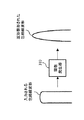
図14は、従来の増幅器において抽出される包絡線が歪む様子を示した説明図である。より具体的には、キャリア増幅器の入力電力対ドレイン電流特性を模式化した特性を示しており、基軸は、縦軸および横軸ともに、リニアスケールである。入力電力対ドレイン電流特性が、特性曲線801の関係を有する場合に、キャリア増幅器に入力電力波形802が入力されると、電流特性803が得られる。
FIG. 14 is an explanatory diagram showing how the envelope extracted in the conventional amplifier is distorted. More specifically, the characteristics of the input power versus drain current characteristics of the carrier amplifier are schematically shown, and the basic axis is a linear scale for both the vertical axis and the horizontal axis. When the input power vs. drain current characteristic has a relationship of a
この電流特性803をキャリア増幅器のドレイン電圧給電回路に設けられた抵抗端から抽出することにより包絡線を得ることができる。しかしながら、電流特性803の中の一部分である特性803aおよび特性803bに示すように、抽出される包絡線には歪みが生じる。
By extracting this
同様に、特許文献1の図1において、検出器が、例えばダイオードなどの非線形特性を持つデバイスを用いて構成された場合、ダイオードの自乗特性により波形が歪むことで、入力信号のダイナミックレンジが得られない問題がある。
Similarly, in FIG. 1 of
これらの問題により、特許文献1の図5A、図5Bに示される制御をキャリア増幅器およびピーク増幅器に適用しても、期待する動作をしない問題があり、効率の低下ないしは歪みを発生させる。このことは、制御信号を生成するための包絡線には歪みが無いことが必要であることを意味し、変調波信号に忠実な包絡線をドレイン電圧給電回路から抽出することが必要とされる。
Due to these problems, there is a problem that even if the control shown in FIGS. 5A and 5B of
本発明は上述のような課題を解決するためになされたもので、あらかじめ期待したバイアス制御が可能となり、効率の低下および歪みの発生を抑えた高効率増幅器を得ることを目的とする。 The present invention has been made to solve the above-described problems, and an object of the present invention is to obtain a high-efficiency amplifier that can control a bias that is expected in advance, and that suppresses a decrease in efficiency and distortion.
本発明に係る高効率増幅器は、RF入力信号に対応する包絡線信号を抽出する包絡線信号抽出手段と、抽出された包絡線信号に基づいてRF入力信号を増幅し、電圧制御信号を生成するための電圧制御器と、電圧制御信号に応じてRF入力信号を増幅する増幅器とを備えた高効率増幅器において、抽出された包絡線信号を入力とし、包絡線信号の波形がRF入力信号の真の包絡線と同等の波形となるように、あらかじめ定められた入出力特性に基づいて波形整形を行い、波形整形後の出力信号を生成する波形整形手段をさらに備え、電圧制御器は、波形整形手段による波形整形後の出力信号に基づいて、バイアスを動的に制御するための電圧制御信号を生成して増幅器を制御するものである。 A high-efficiency amplifier according to the present invention generates an envelope signal extraction unit that extracts an envelope signal corresponding to an RF input signal, amplifies the RF input signal based on the extracted envelope signal, and generates a voltage control signal A high-efficiency amplifier having a voltage controller for amplification and an amplifier that amplifies the RF input signal in accordance with the voltage control signal. The extracted envelope signal is input and the waveform of the envelope signal is the true value of the RF input signal. The waveform controller further includes waveform shaping means for performing waveform shaping based on predetermined input / output characteristics so as to obtain a waveform equivalent to the envelope of the waveform, and generating an output signal after waveform shaping. Based on the output signal after the waveform shaping by the means, a voltage control signal for dynamically controlling the bias is generated to control the amplifier.
本発明によれば、RF入力信号に対応して抽出された歪んだ包絡線信号に対して、波形整形を適用することによって入力信号包絡線を再現することができ、この再現された入力信号包絡線を用いて増幅器のバイアスを制御することにより、あらかじめ期待したバイアス制御が可能となり、効率の低下および歪みの発生を抑えた高効率増幅器を得ることができる。 According to the present invention, an input signal envelope can be reproduced by applying waveform shaping to a distorted envelope signal extracted corresponding to an RF input signal, and the reproduced input signal envelope is reproduced. By controlling the bias of the amplifier using a line, it is possible to control the bias expected in advance, and it is possible to obtain a high-efficiency amplifier with reduced efficiency and distortion.
以下、本発明の高効率増幅器の好適な実施の形態につき図面を用いて説明する。 Hereinafter, preferred embodiments of the high efficiency amplifier of the present invention will be described with reference to the drawings.
実施の形態1.
図1は、本発明の実施の形態1における高効率増幅器の構成図である。この高効率増幅器は、キャリア増幅器101、ピーク増幅器102、電力分配器103、電力合成器104を備えたドハティ増幅器とともに、電圧抽出手段200、波形整形手段300、および電圧制御器400で構成される。ここで、電圧抽出手段200は、包絡線信号抽出手段に相当する。
FIG. 1 is a configuration diagram of a high-efficiency amplifier according to
まず始めに、接続構成について説明する。
電力分配器103は、キャリア増幅器101およびピーク増幅器102の入力に接続される。キャリア増幅器101は、ドレイン給電線路を介してドレイン電圧Vdが供給されるとともに、このドレイン給電線路には電圧抽出手段200が挿入されている。そして、電圧抽出手段200の出力は、波形整形手段300に入力される。
First, the connection configuration will be described.
The
波形整形手段300の出力は、電圧制御器400に入力される。そして、電圧制御器400の出力は、ピーク増幅器102のゲート電圧給電回路に接続される。キャリア増幅器101の出力、およびピーク増幅器102の出力は、電力合成器104に接続される。
The output of the waveform shaping means 300 is input to the
次に、図1に示したドハティ増幅器を含む高効率増幅器の動作について説明する。
信号入力であるRF信号は、電力分配器103によってキャリア増幅器101およびピーク増幅器102に電力分配される。
Next, the operation of the high efficiency amplifier including the Doherty amplifier shown in FIG. 1 will be described.
The RF signal that is a signal input is distributed to the
キャリア増幅器101にRF信号が入力されると、ドレイン電圧給電回路には信号増幅に伴う電流が発生する。これに対して、電圧抽出手段200は、このドレイン電圧給電回路に発生する電流を、微小抵抗値を有する抵抗の両端に発生する電位を差動増幅することにより、包絡線信号に変換する。
When an RF signal is input to the
電圧抽出手段200により抽出された包絡線信号は、波形整形手段300に入力される。波形整形手段300は、入力される包絡線の波形整形を行う。つまり、この波形整形手段300は、RF入力信号と同等の包絡線を再生し、出力することとなる。
The envelope signal extracted by the
より具体的には、波形整形手段300は、電圧抽出手段200により抽出された包絡線信号を入力とし、包絡線信号の波形がRF入力信号の真の包絡線と同等の波形となるような出力が得られるように、あらかじめ定められた入出力特性を図示しない記憶部に有しており、この入出力特性に基づいて波形整形後の出力信号を生成する。なお、波形整形手段300の詳細構成は、実施の形態3〜5で後述する。
More specifically, the
波形整形手段300による波形整形後の出力信号は、電圧制御器400に入力される。そして、電圧制御器400は、例えばピーク増幅器のゲート電圧を動的に制御するための制御信号を生成し、出力する。このとき、電圧制御器400の出力信号は、ピーク増幅器102のゲート電圧給電回路に入力される。
The output signal after the waveform shaping by the waveform shaping means 300 is input to the
以上のように、実施の形態1によれば、キャリア増幅器のドレイン電圧給電回路から得られるRF出力信号の包絡線を波形整形することにより、RF入力信号の包絡線を再生することができる。この結果、忠実な変調波包絡線を基準信号としてバイアスを制御することにより、あらかじめ期待したバイアス制御が可能となり、効率の低下および歪みの発生を抑えた高効率増幅器を得ることができる。 As described above, according to the first embodiment, the envelope of the RF input signal can be reproduced by shaping the envelope of the RF output signal obtained from the drain voltage supply circuit of the carrier amplifier. As a result, by controlling the bias using the faithful modulated wave envelope as a reference signal, it is possible to perform a bias control that is expected in advance, and it is possible to obtain a high-efficiency amplifier with reduced efficiency and distortion.
実施の形態2.
図2は、本発明の実施の形態2における高効率増幅器の構成図である。この高効率増幅器は、前置増幅器111、後置増幅器112を備えた電力増幅器とともに、電圧抽出手段200、波形整形手段300、および電圧制御器400で構成される。ここで、電圧抽出手段200は、包絡線信号抽出手段に相当する。
Embodiment 2. FIG.
FIG. 2 is a configuration diagram of the high efficiency amplifier according to the second embodiment of the present invention. This high-efficiency amplifier is composed of a voltage extraction means 200, a waveform shaping means 300, and a
まず始めに、接続構成について説明する。
前置増幅器111は、ドレイン給電線路を介してドレイン電圧Vdが供給されるとともに、このドレイン給電線路には電圧抽出手段200が挿入されている。そして、電圧抽出手段200の出力は、波形整形手段300に入力される。この電圧抽出手段200および波形整形手段300の構成については、先の実施の形態1と同様である。
First, the connection configuration will be described.
The
さらに、波形整形手段300の出力は、電圧制御器400に入力される。そして、電圧制御器400の出力は、後置増幅器112のゲート電圧給電回路あるいはドレイン電圧給電回路に接続される。
Further, the output of the waveform shaping means 300 is input to the
次に、図2に示した電力増幅器を含む高効率増幅器の動作について説明する。
RF信号が入力されると、前置増幅器111のドレイン電圧給電回路内で信号増幅に伴う電流が発生する。ここで、電圧抽出手段200および波形整形手段300の動作については、先の実施の形態1と同様である。
Next, the operation of the high efficiency amplifier including the power amplifier shown in FIG. 2 will be described.
When the RF signal is input, a current accompanying signal amplification is generated in the drain voltage supply circuit of the
さらに、電圧制御器400の出力信号は、後置増幅器112の電圧給電回路に入力され、後置増幅器112のバイアスを動的に制御する。
Further, the output signal of the
以上のように、実施の形態2によれば、前置増幅器のドレイン電圧給電回路から得られるRF出力信号の包絡線を波形整形することにより、RF入力信号の包絡線を再生することができる。この結果、忠実な変調波包絡線を基準信号として後置増幅器のバイアスを制御することにより、あらかじめ期待したバイアス制御が可能となり、効率の低下および歪みの発生を抑えた高効率増幅器を得ることができる。 As described above, according to the second embodiment, the envelope of the RF input signal can be reproduced by shaping the waveform of the RF output signal obtained from the drain voltage supply circuit of the preamplifier. As a result, by controlling the bias of the post-amplifier using the faithful modulation wave envelope as a reference signal, it is possible to control the bias expected in advance, and it is possible to obtain a high-efficiency amplifier with reduced efficiency and distortion. it can.
さらに、前置増幅器のドレイン電圧給電回路に電圧抽出手段を持つことで、先の実施の形態1と比較して、電圧抽出手段で発生する電力損失を小さく、すなわち、系全体での電力損失を小さくすることができる。 Further, by having the voltage extraction means in the drain voltage supply circuit of the preamplifier, the power loss generated in the voltage extraction means is smaller than in the first embodiment, that is, the power loss in the entire system is reduced. Can be small.
実施の形態3.
本実施の形態3では、波形整形手段300の具体例として、関数発生器を適用した場合について説明する。図3は、本発明の実施の形態3における関数発生器の処理を説明するための図である。この図3において、入力される包絡線波形は、整形を行うための関数・特性を保持する関数発生器310により、RF入力信号包絡線を再生するように包絡線波形を出力する。
In the third embodiment, a case where a function generator is applied will be described as a specific example of the waveform shaping means 300. FIG. 3 is a diagram for explaining the processing of the function generator in the third embodiment of the present invention. In FIG. 3, the envelope waveform that is input is output as an envelope waveform so as to reproduce the RF input signal envelope by the
すなわち、関数発生器310は、電圧抽出手段200により抽出された包絡線信号を入力とし、包絡線信号の波形がRF入力信号の真の包絡線と同等の波形となるような出力が得られるように、あらかじめ定められた入出力特性あるいは関数を図示しない記憶部に保持しておくことにより、この入出力特性に基づいて波形整形後の出力信号を生成できる。
That is, the
以上のように、実施の形態3によれば、所定の入出力特性あるいは関数を備えた関数発生器による波形整形により、出力電流波形の電流特性から得られる包絡線歪みを伴う包絡線は補正され、RF入力信号波形の包絡線と同等とすることが可能となる。この結果、忠実な変調波包絡線を基準信号としてバイアスを制御することにより、あらかじめ期待したバイアス制御が可能となり、効率の低下および歪みの発生を抑えた高効率増幅器を得ることができる。 As described above, according to the third embodiment, the envelope with the envelope distortion obtained from the current characteristic of the output current waveform is corrected by the waveform shaping by the function generator having a predetermined input / output characteristic or function. It becomes possible to make it equivalent to the envelope of the RF input signal waveform. As a result, by controlling the bias using the faithful modulated wave envelope as a reference signal, it is possible to perform a bias control that is expected in advance, and it is possible to obtain a high-efficiency amplifier with reduced efficiency and distortion.
実施の形態4.
図4は、本発明の実施の形態4における関数発生器の構成図、および波形整形の説明図である。この関数発生器310は、非線形素子であるダイオード、抵抗器およびオペアンプから構成される。図4の構成において、回路定数R1〜R6、Vb、適切なダイオードD1およびD2を定めることにより、所望関数の近似を行う(例えば、「OPアンプの回路設計」、岡村廸夫、CQ出版、1973参照)。
FIG. 4 is a configuration diagram of a function generator and an explanatory diagram of waveform shaping in the fourth embodiment of the present invention. The
次に、図4に示した関数発生器310による波形整形の動作について説明する。
例えば、図4の波形整形の説明図に示すように、回路定数R1〜R6、Vb、適切なダイオードD1およびD2を定めることにより、歪み波形L1の入力に対して、逆特性波形L3を発生させることができ、その結果、無歪み波形特性L2を出力信号として得ることができる。
Next, the waveform shaping operation by the
For example, as shown in the waveform shaping explanatory diagram of FIG. 4, by defining circuit constants R1 to R6, Vb and appropriate diodes D1 and D2, an inverse characteristic waveform L3 is generated with respect to the input of the distortion waveform L1. As a result, the undistorted waveform characteristic L2 can be obtained as an output signal.
以上のように、実施の形態4によれば、大信号時における歪み波形特性は、関数発生器が有する逆特性により波形整形され、無歪み波形特性に補正することが可能となる。この結果、忠実な変調波包絡線を基準信号としてバイアスを制御することにより、あらかじめ期待したバイアス制御が可能となり、効率の低下および歪みの発生を抑えた高効率増幅器を得ることができる。 As described above, according to the fourth embodiment, the distortion waveform characteristic at the time of a large signal is shaped by the inverse characteristic of the function generator and can be corrected to the distortion-free waveform characteristic. As a result, by controlling the bias using the faithful modulated wave envelope as a reference signal, it is possible to perform a bias control that is expected in advance, and it is possible to obtain a high-efficiency amplifier with reduced efficiency and distortion.
実施の形態5.
図5は、本発明の実施の形態5におけるデジタル信号処理技術を用いた波形整形手段および電圧制御器の構成図である。図5に示す回路は、波形整形手段300および電圧制御器400の機能を兼ね備えており、A/Dコンバータ321、デジタル信号処理手段322、およびD/Aコンバータ323で構成される。
Embodiment 5. FIG.
FIG. 5 is a configuration diagram of the waveform shaping means and the voltage controller using the digital signal processing technique according to the fifth embodiment of the present invention. The circuit shown in FIG. 5 has the functions of the
次に、図5に示した回路の動作について説明する。
A/Dコンバータ321は、先の図1の電圧抽出手段200の出力である包絡線信号を取り込み、量子化する。量子化された信号は、デジタル信号処理手段322に入力され、波形整形が行われる。この波形整形によりRF信号包絡線が再生される。この包絡線を基準信号としてゲート電圧制御信号がさらに生成され、D/Aコンバータ323に出力される。
Next, the operation of the circuit shown in FIG. 5 will be described.
The A /
このデジタル信号処理手段322は、所定の入出力特性あるいは関数を、例えば、補正テーブルデータとしてあらかじめ保持しておくことにより、歪みを伴う包絡線をデジタル的に補正することができる。さらに、デジタル信号処理手段322は、補正後の包絡線信号からゲート電圧制御信号を生成することができ、電圧制御器400の機能を併せ持つことができる。
The digital signal processing means 322 can digitally correct an envelope with distortion by holding predetermined input / output characteristics or functions in advance as, for example, correction table data. Further, the digital signal processing means 322 can generate a gate voltage control signal from the corrected envelope signal, and can also have the function of the
以上のように、実施の形態5によれば、デジタル信号処理手段を用いることにより、波形整形手段の機能と電圧制御器の機能の両方を実現できる。この結果、波形整形回路と電圧制御回路を一つのデジタル回路に集約することができ、効率・歪に対し、改善効果を与えることが可能となる。 As described above, according to the fifth embodiment, both the function of the waveform shaping unit and the function of the voltage controller can be realized by using the digital signal processing unit. As a result, the waveform shaping circuit and the voltage control circuit can be integrated into one digital circuit, and an improvement effect can be given to efficiency and distortion.
実施の形態6.
本実施の形態6では、図1における電圧抽出手段200または図2における電圧抽出手段200の具体的な構成について説明する。図6は、本発明の実施の形態6における電圧抽出手段の構成図である。この電圧抽出手段200は、低周波デカップリング部201、電圧検出抵抗器202、高調波反射ネットワーク部203、電圧検出端204、および差動増幅器205で構成される。ここで、低周波デカップリング部201は、低周波デカップリング回路に相当し、高調波反射ネットワーク部203は、高調波反射回路に相当する。
Embodiment 6 FIG.
In the sixth embodiment, a specific configuration of the
次に、図6に示した電圧抽出手段200の動作について説明する。
電圧検出抵抗器202は、図1におけるキャリア増幅器101のドレイン電圧給電回路に発生する電流を電圧変換する。電圧検出端204は、電圧検出抵抗器202の両端に接続され、包絡線電圧を電位”Vdet+”および“Vdet−”で出力する。さらに、差動増幅器205は、この電位を電位差”Vdet+”−“Vdet−”に変換して出力する。
Next, the operation of the
The
ここで、低周波デカップリング部201は、電源およびFET端からの低周波信号をブロックするために配置される。また、高調波反射ネットワーク部203は、増幅器であるFET端からのRF信号および高調波をブロックするために配置される。
Here, the low-
以上のように、実施の形態6によれば、電圧抽出手段が低周波デカップリング回路および高調波反射回路を備えることにより、包絡線波形から不要周波数成分を除去することができ、不要周波数成分除去のための濾波器を削減することができる。 As described above, according to the sixth embodiment, the voltage extraction unit includes the low-frequency decoupling circuit and the harmonic reflection circuit, so that unnecessary frequency components can be removed from the envelope waveform, and unnecessary frequency component removal is performed. The filter for can be reduced.
実施の形態7.
本実施の形態7では、電圧抽出手段に対して、さらに電圧オフセット手段を導入する場合について説明する。図7は、本発明の実施の形態7における電圧オフセット手段の具体的な構成図である。図7における電圧抽出手段200aは、トランスを用いて絶対電圧値を降下させた場合を例示している。また、図7における電圧抽出手段200bは、抵抗分圧を利用して絶対電圧を降下させた場合を例示している。さらに、図7における電圧抽出手段200cは、オペアンプの電源電圧にオフセット電圧を印加した場合を例示している。
Embodiment 7 FIG.
In the seventh embodiment, a case where a voltage offset unit is further introduced to the voltage extracting unit will be described. FIG. 7 is a specific block diagram of the voltage offset means in the seventh embodiment of the present invention. The voltage extraction means 200a in FIG. 7 illustrates the case where the absolute voltage value is lowered using a transformer. Moreover, the voltage extraction means 200b in FIG. 7 illustrates the case where the absolute voltage is lowered using resistance voltage division. Furthermore, the voltage extraction means 200c in FIG. 7 illustrates the case where an offset voltage is applied to the power supply voltage of the operational amplifier.
次に、このような電圧オフセット手段を有する電圧抽出手段の動作について説明する。
図7に示すいずれの回路においても、電圧オフセット手段の働きにより、電圧検出端204にて得られた絶対電位”Vdet+”および“−Vdet”を下げて、包絡線信号を得ることができる。
Next, the operation of the voltage extracting means having such a voltage offset means will be described.
In any of the circuits shown in FIG. 7, the envelope signal can be obtained by lowering the absolute potentials “Vdet +” and “−Vdet” obtained at the
以上のように、実施の形態7によれば、例えば、キャリア増幅器のトランジスタがLDMOSトランジスタやGaNトランジスタである場合、ドレイン給電部に印加する電源電圧は、約数十Vであり、電圧抽出手段から得られる電圧値は、電圧検出端204の絶対電圧”Vdet+”および“Vdet−”から約数十Vで取り出さなければならない。したがって、このような場合にも、図7に示す電圧オフセット回路を用いることにより、絶対電位をさげることができ、電圧検出端204に接続されるデバイスの選定が容易になる。
As described above, according to the seventh embodiment, for example, when the transistor of the carrier amplifier is an LDMOS transistor or a GaN transistor, the power supply voltage applied to the drain power supply unit is about several tens of volts, The obtained voltage value must be taken out from the absolute voltages “Vdet +” and “Vdet−” of the
実施の形態8.
本実施の形態8では、図1における電圧制御器400の具体的な構成について説明する。図8は、本発明の実施の形態8における電圧制御器400の具体例な構成図である。本回路は、スイッチング動作を行うコンパレータ401を備えている。
Embodiment 8 FIG.
In the eighth embodiment, a specific configuration of the
このようなコンパレータ401を有する電圧制御器400は、スイッチング手段以外にも、目的に合わせて他の手段、例えば、3値以上の多値切り替えや、シームレスかつ線形にゲート電圧を印加、シームレスかつ包絡線電圧値に対して重み付けするような非線形特性を持たせたゲート電圧として印加する制御方法を選択することができる。
In addition to the switching means, the
次に、このような電圧制御器400がゲート電圧を制御する場合の具体的な動作について説明する。
理想的な2−WAYドハティ増幅器は、飽和出力からのバックオフ量が6dB以上において、ピーク増幅器の電流を消費しない。
Next, a specific operation when such a
An ideal 2-WAY Doherty amplifier does not consume the peak amplifier current when the backoff amount from the saturated output is 6 dB or more.
しかしながら、実際にはピーク増幅器に適用されるトランジスタの特性、ピーク増幅器のゲート電圧値およびピーク増幅器の入出力整合条件等により、バックオフ量6dB以上の地点においてもピーク増幅器の電流は消費する。バックオフ量6dB以上でのピーク増幅器の出力電力は、キャリア増幅器の出力電力と比較して非常に小さく有効に利用されない。このため、ピーク増幅器の消費電流は、ドハティ増幅器の効率低下に直結する。 However, the current of the peak amplifier is consumed even at a point where the back-off amount is 6 dB or more depending on the characteristics of the transistor applied to the peak amplifier, the gate voltage value of the peak amplifier, and the input / output matching conditions of the peak amplifier. The output power of the peak amplifier with a back-off amount of 6 dB or more is very small compared to the output power of the carrier amplifier and cannot be used effectively. For this reason, the consumption current of the peak amplifier is directly linked to a decrease in efficiency of the Doherty amplifier.
このことから、小・中信号領域におけるピーク増幅器の消費電流を削減し、効率を向上させる必要がある。例えば、特許文献1の図5Aおよび図5Bに示された従来の制御のように、入力電力に比例したあるゲート電圧を印加したときには、立ち上がりが急峻である理想的なC級動作を実現することができない。すなわち、切替え点付近でピーク増幅器が電流を消費することとなる。
Therefore, it is necessary to reduce the current consumption of the peak amplifier in the small / medium signal region and improve the efficiency. For example, as in the conventional control shown in FIGS. 5A and 5B of
このような場合に対して、スイッチング制御を適用することで、ピーク増幅器のゲート電圧をON/OFF切替えして理想的なC級動作に近づけることができ、その結果として、切替え点まで電流を削減することができる。 In such a case, by applying switching control, the gate voltage of the peak amplifier can be switched ON / OFF to approach an ideal class C operation, and as a result, the current is reduced to the switching point. can do.
図9は、本発明の実施の形態8におけるコンパレータの動作の説明図である。コンパレータ401は、波形整形手段300の出力信号が入力されると、閾値電圧Vthを基準として、包絡線電圧404が閾値電圧Vthより小さい場合は、ローレベル判定し、大きい場合にはハイレベル判定する。
FIG. 9 is an explanatory diagram of the operation of the comparator in the eighth embodiment of the present invention. When the output signal of the waveform shaping means 300 is input, the
ここでいうローレベル判定とは、ピーク増幅器102のゲート電圧を切り下げる制御信号を出力することを意味する。一方、ハイレベル判定とは、ピーク増幅器102のゲート電圧を切り上げる制御信号を出力することを意味する。
Here, the low level determination means that a control signal for reducing the gate voltage of the
この閾値電圧Vthの決定方法の一例を、図9に基づいて説明する。包絡線電圧404の最大瞬時電力点に対応する最大電圧値405を把握し、あらかじめ定めた切替えバックオフ量406から切替え電圧値403を求める。この切替え電圧値403がコンパレータ401の閾値電圧Vthとなる。
An example of a method for determining the threshold voltage Vth will be described with reference to FIG. A
コンパレータ401がピーク増幅器102のゲート電圧給電回路を駆動する能力がない場合、コンパレータ401の出力は、ゲート電圧給電回路を駆動する能力を有するゲート電圧ドライバに接続してもよい。
If the
そこで、ゲート電圧ドライバを接続した場合の動作について、次に説明する。ゲート電圧ドライバは、ゲート電圧制御器としてコンパレータ401が採用された場合、コンパレータ401が出力するローレベル判定およびハイレベル判定によりスイッチング動作をする。
The operation when the gate voltage driver is connected will be described next. When the
ローレベル判定の場合、ピーク増幅器の消費電流を削減する観点から、ピンチオフ電圧より充分小さいこと、かつドハティ増幅器バックオフ量が6dB以上において電流を消費しないことを満たすゲート電圧値(Vg=Vlo)が出力される。 In the case of the low level determination, from the viewpoint of reducing the current consumption of the peak amplifier, a gate voltage value (Vg = Vlo) satisfying that it is sufficiently smaller than the pinch-off voltage and does not consume current when the Doherty amplifier back-off amount is 6 dB or more Is output.
ハイレベル判定の場合、ドハティ増幅器の飽和電力、動作点での効率・歪みの三者を比較することにより、最適化されたゲート電圧値(Vg=Vhi)が出力される。このときのゲート電圧Vgの関係は、Vlo<Vhiであり、ドハティ増幅器の瞬時飽和電力は、ピーク増幅器のゲート電圧Vg=Vhiに固定設定した場合のドハティ増幅器の瞬時飽和電力に一致する。 In the case of high level determination, an optimized gate voltage value (Vg = Vhi) is output by comparing the saturation power of the Doherty amplifier and the efficiency / distortion at the operating point. The relationship of the gate voltage Vg at this time is Vlo <Vhi, and the instantaneous saturation power of the Doherty amplifier matches the instantaneous saturation power of the Doherty amplifier when the gate voltage Vg of the peak amplifier is fixed to Vhi.
図1の電圧制御器400は、スイッチング手段以外にも、目的に合わせて他の手段を選択することができる。図8に示した本実施の形態8は、効率を優先した例である。ドハティ増幅器の線形性を優先する場合、この変調波包絡線電圧値を基に、ピーク増幅器102のゲート電圧を3値以上に多値切替えすることや、シームレスかつ線形にゲート電圧を印加、または、シームレスかつ包絡線電圧値に対して重み付けしてするような非線形特性をゲート電圧として印加する制御方法を採用してもよい。
The
以上のように、実施の形態8によれば、波形整形手段から得られる波形によりバイアスを制御することで、効率・歪に対し、改善効果を与えることが可能となる。さらに、バイアス制御にスイッチング手段を用いれば、ピーク増幅器は、理想的なC級動作に近づくことによって、ピーク増幅器のON、OFF動作を実現し、切替え点まで電流を削減でき、従来の制御より高効率とすることができる。 As described above, according to the eighth embodiment, it is possible to provide an improvement effect on efficiency and distortion by controlling the bias with the waveform obtained from the waveform shaping means. Furthermore, if switching means is used for bias control, the peak amplifier can achieve ON / OFF operation of the peak amplifier by approaching an ideal class C operation, and the current can be reduced to the switching point, which is higher than conventional control. It can be efficiency.
実施の形態9.
本実施の形態9では、先の実施の形態2における図2の高効率増幅器において、後置増幅器112としてドハティ増幅器を配置した場合について説明する。この構成において、電圧制御器400は、キャリア増幅器またはピーク増幅器のゲート電圧給電回路に接続される。
Embodiment 9 FIG.
In the ninth embodiment, a case where a Doherty amplifier is arranged as the post-amplifier 112 in the high efficiency amplifier of FIG. 2 in the second embodiment will be described. In this configuration, the
次に、ドハティ増幅器を用いた高効率増幅器の動作について説明する。
例えば、ピーク増幅器側のゲート電圧給電回路にドハティ増幅器を接続した場合には、先の実施の形態1と同等の動作をする
Next, the operation of the high efficiency amplifier using the Doherty amplifier will be described.
For example, when a Doherty amplifier is connected to the gate voltage supply circuit on the peak amplifier side, the same operation as in the first embodiment is performed.
以上のように、実施の形態9によれば、後置増幅器としてドハティ増幅器を用いることにより、前置増幅器のドレイン電圧給電回路から得られるRF出力信号の包絡線を波形整形して、RF入力信号の包絡線を再生することができる。この結果、忠実な変調波包絡線を基準信号としてバイアスを制御することが可能となる。 As described above, according to the ninth embodiment, by using a Doherty amplifier as a post-amplifier, an RF output signal envelope obtained from the drain voltage supply circuit of the pre-amplifier is waveform-shaped, and the RF input signal The envelope can be regenerated. As a result, the bias can be controlled using the faithful modulation wave envelope as a reference signal.
実施の形態10.
本実施の形態10では、上述した実施の形態9と同様に、先の実施の形態2における図2の高効率増幅器において、後置増幅器112としてドハティ増幅器を配置した場合について説明する。本実施の形態10の構成において、電圧制御器400は、キャリア増幅器またはピーク増幅器のドレイン電圧給電回路に接続される。
Embodiment 10 FIG.
In the tenth embodiment, a case where a Doherty amplifier is arranged as the post-amplifier 112 in the high efficiency amplifier of FIG. In the configuration of the tenth embodiment,
次に、ドハティ増幅器を用いた高効率増幅器の動作について説明する。
本実施の形態10において、後置増幅器112のドレイン電圧は、先の実施の形態1と同様に制御される。
Next, the operation of the high efficiency amplifier using the Doherty amplifier will be described.
In the tenth embodiment, the drain voltage of the post-amplifier 112 is controlled in the same manner as in the first embodiment.
以上のように、実施の形態10によれば、後置増幅器としてドハティ増幅器を用いることにより、前置増幅器のドレイン電圧給電回路から得られるRF出力信号の包絡線を波形整形して、RF入力信号の包絡線を再生することができる。この結果、忠実な変調波包絡線を基準信号としてバイアスを制御することが可能となる効果が得られる。 As described above, according to the tenth embodiment, the envelope of the RF output signal obtained from the drain voltage supply circuit of the preamplifier is shaped by using the Doherty amplifier as the postamplifier, and the RF input signal The envelope can be regenerated. As a result, it is possible to control the bias using a faithful modulated wave envelope as a reference signal.
実施の形態11.
本実施の形態11では、先の実施の形態2における図2の高効率増幅器において、後置増幅器112としてトランジスタ1個で構成された単体増幅器を配置した場合について説明する。この構成において、電圧制御器400は、単体増幅器のドレイン電圧給電回路に接続される。
Embodiment 11 FIG.
In the eleventh embodiment, a case will be described in which a single amplifier constituted by one transistor is arranged as the post-amplifier 112 in the high efficiency amplifier of FIG. 2 in the second embodiment. In this configuration, the
次に、単体増幅器を用いた高効率増幅器の動作について説明する。
本実施の形態11において、後置増幅器112のドレイン電圧は、先の実施の形態1と同様に制御される。
Next, the operation of a high efficiency amplifier using a single amplifier will be described.
In the eleventh embodiment, the drain voltage of the post-amplifier 112 is controlled in the same manner as in the first embodiment.
以上のように、実施の形態11によれば、後置増幅器として単体増幅器を用いることにより、前置増幅器111のドレイン電圧給電回路から得られるRF出力信号の包絡線を波形整形して、RF入力信号の包絡線を再生することができる。この結果、忠実な変調波包絡線を基準信号としてバイアスを制御することが可能となる効果が得られる。
As described above, according to the eleventh embodiment, by using a single amplifier as a post-amplifier, the envelope of the RF output signal obtained from the drain voltage supply circuit of the
実施の形態12.
本実施の形態12では、先の実施の形態1における図1、あるいは先の実施の形態2における図2の高効率増幅器において、波形整形手段300が、入力信号包絡線を利用するサブシステム500にさらに接続される場合について説明する。図10は、本発明の実施の形態12におけるサブシステムに接続された高効率増幅器の構成図であり、波形整形手段300は、サブシステム500に接続されている。
Embodiment 12 FIG.
In the twelfth embodiment, in the high efficiency amplifier of FIG. 1 in the previous first embodiment or in FIG. 2 in the previous second embodiment, the waveform shaping means 300 is added to the
次に、サブシステム500に接続された高効率増幅器の動作について説明する。
波形整形手段300に相当する波形整形手段300の出力信号は、サブシステム500に供給される。このような接続構成により、高効率増幅器内のサブシステム500が、波形整形後の出力信号を必要としている場合には、波形整形手段300から供給することができる。
Next, the operation of the high efficiency amplifier connected to the
An output signal of the
以上のように、実施の形態12によれば、波形整形後の出力信号を必要とするサブシステムが高効率増幅器内にある場合にも、波形整形手段から波形整形後の出力信号を供給することにより入力信号の包絡線が再生される。この結果、サブシステムとして、例えば、電力モニタに接続する際にも、精度の高い電力の計測を可能にする。 As described above, according to the twelfth embodiment, even when a subsystem that requires an output signal after waveform shaping is in the high efficiency amplifier, the output signal after waveform shaping is supplied from the waveform shaping means. Thus, the envelope of the input signal is reproduced. As a result, when the subsystem is connected to, for example, a power monitor, the power can be measured with high accuracy.
実施の形態13.
図11は、本発明の実施の形態13における高効率増幅器の構成図である。この高効率増幅器は、キャリア増幅器101、ピーク増幅器102、電力分配器103、電力合成器104を備えたドハティ増幅器とともに、電圧制御器400a、400b、波形整形手段300、入力分配手段600、および検波回路210で構成される。ここで、検波回路210は、包絡線信号抽出手段に相当する。
Embodiment 13 FIG.
FIG. 11 is a configuration diagram of the high efficiency amplifier according to the thirteenth embodiment of the present invention. This high efficiency amplifier includes a
まず始めに、接続構成について説明する。
入力分配手段600は、電力分配器103および検波回路210に接続される。検波回路210は、例えば、ダイオード、時定数回路、フィルタ等で構成される。検波回路210の出力は、キャリア増幅器101の電圧制御器400aあるいはピーク増幅器102の電圧制御器400bに接続される。
First, the connection configuration will be described.
Input distribution means 600 is connected to
電圧制御器400aの出力は、キャリア増幅器101の電圧給電回路に接続される。電圧制御器400bの出力は、キャリア増幅器101の電圧給電回路に接続される。電力分配器103は、キャリア増幅器101とピーク増幅器102の入力に接続される。そして、キャリア増幅器101の出力とピーク増幅器102の出力は電力合成器104に接続される。
The output of the
次に、図11に示したドハティ増幅器を含む高効率増幅器の動作について説明する。
入力信号であるRF信号は、入力分配手段600によって電力分配器103および検波回路210に分配される。
Next, the operation of the high efficiency amplifier including the Doherty amplifier shown in FIG. 11 will be described.
An RF signal that is an input signal is distributed to the
検波回路210は、入力されたRF信号から包絡線信号を抽出し、抽出された包絡線信号は、波形整形手段300に入力される。波形整形手段300は、入力される包絡線信号の波形整形を行う。つまり、この波形整形手段300は、RF入力信号と同等の包絡線を再生し、出力することとなる。なお、波形整形手段300としては、例えば、先の実施の形態4に示す図4の回路が適用できる。
The
波形整形手段300の出力信号は、キャリア増幅器101の電圧制御器400aおよびピーク増幅器102の電圧制御器400bに入力される。電圧制御器400aおよび400bは、バイアスを動的に制御するための制御信号を生成し、出力する。また、波形整形手段300と電圧制御器400aと電圧制御器400bは、先の実施の形態5に示す図5の回路のように、デジタル信号処理技術を適用することも可能である。
The output signal of the waveform shaping means 300 is input to the
電圧制御器400aの出力信号は、キャリア増幅器101の電圧給電回路に入力される。電圧制御器400bの出力信号は、ピーク増幅器102の電圧給電回路に入力される。なお、図11においては、2つの電圧制御器400a、400bを用いているが、これらをまとめた1台の電圧制御器で構成することも可能である。
The output signal of the
以上のように、実施の形態13によれば、検波回路から得られる包絡線を波形整形することにより、RF入力信号の包絡線を再生することができる。この結果、忠実な変調波包絡線を基準信号としてドハティ増幅器のバイアスを制御することが可能となる。 As described above, according to the thirteenth embodiment, the envelope of the RF input signal can be reproduced by shaping the envelope obtained from the detection circuit. As a result, the bias of the Doherty amplifier can be controlled using the faithful modulation wave envelope as a reference signal.
実施の形態14.
本実施の形態14では、先の実施の形態2における図2の高効率増幅器において、前置増幅器と後置増幅器との間に遅延調整手段を備えた場合について説明する。図12は、本発明の実施の形態14における高効率増幅器の構成図である。この高効率増幅器は、前置増幅器111、後置増幅器112を備えた電力増幅器とともに、遅延調整手段700で構成される。
Embodiment 14 FIG.
In the fourteenth embodiment, a case will be described in which the high-efficiency amplifier in FIG. FIG. 12 is a configuration diagram of the high efficiency amplifier according to the fourteenth embodiment of the present invention. This high-efficiency amplifier is composed of a delay adjustment means 700 together with a power amplifier including a
まず始めに、接続構成について説明する。
本構成は、先の実施の形態2に対して施されたものであり、先の実施の形態2との相違は、前置増幅器111と後置増幅器112との間に遅延調整手段700が挿入された点である。
First, the connection configuration will be described.
This configuration is applied to the previous embodiment 2. The difference from the previous embodiment 2 is that the delay adjusting means 700 is inserted between the
次に、図12に示した高効率増幅器の動作について説明する。
図12に示す前置増幅器111と後置増幅器112との間に遅延調整手段700を挿入することにより、図2の電圧抽出手段200、波形整形手段300および電圧制御器400で生じる遅延時間を補償することができる。
Next, the operation of the high efficiency amplifier shown in FIG. 12 will be described.
By inserting a
以上のように、実施の形態14によれば、遅延調整回路を挿入することにより、先の実施の形態2と比較して、RF信号波形と後置増幅器に印加される電圧制御信号との間に精度の高い同期が確保できる。 As described above, according to the fourteenth embodiment, by inserting a delay adjustment circuit, the RF signal waveform and the voltage control signal applied to the post-amplifier are compared with those in the second embodiment. Highly accurate synchronization can be ensured.
実施の形態15.
本実施の形態15では、先の実施の形態13における図11の高効率増幅器において、さらに遅延調整手段を備えた場合について説明する。図13は、本発明の実施の形態15における高効率増幅器の構成図である。この高効率増幅器は、図11と比較すると、入力分配手段600と電力分配器103との間に遅延調整手段700aをさらに備えている点が異なる。
Embodiment 15 FIG.
In the fifteenth embodiment, a case will be described in which the high efficiency amplifier of FIG. 11 in the previous thirteenth embodiment is further provided with delay adjusting means. FIG. 13 is a configuration diagram of the high efficiency amplifier according to the fifteenth embodiment of the present invention. This high-efficiency amplifier is different from FIG. 11 in that a delay adjusting means 700 a is further provided between the input distribution means 600 and the
なお、この遅延調整手段700aの代わりに、電力分配器103とキャリア増幅器101との間、および電力分配器103とピーク増幅器102との間に遅延調整手段700bを挿入する構成とすることも可能である。
Instead of this delay adjusting means 700a, it is also possible to adopt a configuration in which delay adjusting means 700b is inserted between
次に、図13に示した高効率増幅器の動作について説明する。
図13が示す遅延調整手段700aまたは700bを挿入するにより、図11の波形整形手段300、および電圧制御器400a、400bで生じる遅延時間を、補償することができる。
Next, the operation of the high efficiency amplifier shown in FIG. 13 will be described.
By inserting the delay adjusting means 700a or 700b shown in FIG. 13, the delay time generated in the waveform shaping means 300 and the
以上のように、実施の形態15によれば、遅延調整回路を挿入することにより、先の実施の形態13と比較して、RF信号波形と、キャリア増幅器およびピーク増幅器に印加される電圧制御信号との間に精度の高い同期が確保できる。 As described above, according to the fifteenth embodiment, by inserting a delay adjustment circuit, compared with the previous thirteenth embodiment, the RF signal waveform and the voltage control signal applied to the carrier amplifier and the peak amplifier. Highly accurate synchronization can be ensured between
101 キャリア増幅器、102 ピーク増幅器、103 電力分配器、104 電力合成器、111 前置増幅器、112 後置増幅器、200、200a、200b、200c 電圧抽出手段(包絡線信号抽出手段)、201 低周波デカップリング部(低周波デカップリング回路)、202 電圧検出抵抗器、203 高調波反射ネットワーク部(高調波反射回路)、204 電圧検出端、205 差動増幅器、210 検波回路(包絡線信号抽出手段)、300 波形整形手段、310 関数発生器、321 コンバータ、322 デジタル信号処理手段、323 コンバータ、400、400a、400b 電圧制御器、401 コンパレータ、500 サブシステム、600 入力分配手段、700、700a、700b 遅延調整手段。
DESCRIPTION OF
Claims (14)
抽出された前記包絡線信号に基づいて前記RF入力信号を増幅し、電圧制御信号を生成するための電圧制御器と、
前記電圧制御信号に応じて前記RF入力信号を増幅する増幅器と
を備えた高効率増幅器において、
抽出された前記包絡線信号を入力とし、前記包絡線信号の波形が前記RF入力信号の真の包絡線と同等の波形となるように、あらかじめ定められた入出力特性に基づいて波形整形を行い、波形整形後の出力信号を生成する波形整形手段をさらに備え、
前記電圧制御器は、前記波形整形手段による前記波形整形後の出力信号に基づいて、バイアスを動的に制御するための電圧制御信号を生成して前記増幅器を制御する
ことを特徴とする高効率増幅器。 An envelope signal extracting means for extracting an envelope signal corresponding to the RF input signal;
A voltage controller for amplifying the RF input signal based on the extracted envelope signal and generating a voltage control signal;
A high efficiency amplifier comprising: an amplifier that amplifies the RF input signal in response to the voltage control signal;
Using the extracted envelope signal as an input, waveform shaping is performed based on predetermined input / output characteristics so that the waveform of the envelope signal is equivalent to the true envelope of the RF input signal , Further comprising waveform shaping means for generating an output signal after waveform shaping,
The voltage controller controls the amplifier by generating a voltage control signal for dynamically controlling a bias based on the output signal after the waveform shaping by the waveform shaping unit. amplifier.
前記増幅器は、キャリア増幅器およびピーク増幅器を有するドハティ増幅器で構成され、
前記包絡線信号抽出手段は、前記キャリア増幅器にドレイン電圧を印加するドレイン電圧給電回路に挿入された電圧検出抵抗器を有し、前記電圧検出抵抗器の両端の電圧から前記RF入力信号に対応する包絡線信号を抽出し、
前記電圧制御器は、前記波形整形手段による前記波形整形後の出力信号に基づいて、バイアスを動的に制御するための電圧制御信号を生成して前記ピーク増幅器を制御する
ことを特徴とする高効率増幅器。 The high efficiency amplifier of claim 1.
The amplifier comprises a Doherty amplifier having a carrier amplifier and a peak amplifier,
The envelope signal extraction means has a voltage detection resistor inserted in a drain voltage supply circuit that applies a drain voltage to the carrier amplifier, and corresponds to the RF input signal from the voltage across the voltage detection resistor. Extract the envelope signal,
The voltage controller generates a voltage control signal for dynamically controlling a bias based on the output signal after the waveform shaping by the waveform shaping means, and controls the peak amplifier. Efficiency amplifier.
前記電圧制御器は、前記波形整形手段による前記波形整形後の出力信号と、所定の閾値との比較結果に応じて、バイアスを動的に制御するための電圧制御信号を生成して前記ピーク増幅器を制御することを特徴とする高効率増幅器。 The high efficiency amplifier of claim 2,
The voltage controller generates a voltage control signal for dynamically controlling a bias in accordance with a comparison result between the output signal after the waveform shaping by the waveform shaping unit and a predetermined threshold, and the peak amplifier A high efficiency amplifier characterized by controlling.
前記増幅器は、前置増幅器および後置増幅器を有する電力増幅器で構成され、
前記包絡線信号抽出手段は、前記前置増幅器にドレイン電圧を印加するドレイン電圧給電回路に挿入された電圧検出抵抗器を有し、前記電圧検出抵抗器の両端の電圧から前記RF入力信号に対応する包絡線信号を抽出し、
前記電圧制御器は、前記波形整形手段による前記波形整形後の出力信号に基づいて、バイアスを動的に制御するための電圧制御信号を生成して前記後置増幅器を制御する
ことを特徴とする高効率増幅器。 The high efficiency amplifier of claim 1.
The amplifier comprises a power amplifier having a preamplifier and a postamplifier,
The envelope signal extraction means has a voltage detection resistor inserted in a drain voltage supply circuit that applies a drain voltage to the preamplifier, and corresponds to the RF input signal from the voltage at both ends of the voltage detection resistor. Extract the envelope signal
The voltage controller generates a voltage control signal for dynamically controlling a bias based on the output signal after the waveform shaping by the waveform shaping means, and controls the post-amplifier. High efficiency amplifier.
前記前置増幅器と前記後置増幅器との間に遅延時間の補償を行う遅延調整手段をさらに備えることを特徴とする高効率増幅器。 The high efficiency amplifier according to claim 4.
A high-efficiency amplifier, further comprising delay adjusting means for compensating a delay time between the preamplifier and the postamplifier.
前記後置増幅器は、キャリア増幅器およびピーク増幅器を有するドハティ増幅器で構成され、
前記電圧制御器は、前記ドハティ増幅器内の前記キャリア増幅器または前記ピーク増幅器の、ゲート電圧給電回路またはドレイン電圧給電回路に接続され、前記後置増幅器を制御する
ことを特徴とする高効率増幅器。 The high efficiency amplifier according to claim 4 or 5,
The post-amplifier is composed of a Doherty amplifier having a carrier amplifier and a peak amplifier,
The high-efficiency amplifier, wherein the voltage controller is connected to a gate voltage supply circuit or a drain voltage supply circuit of the carrier amplifier or the peak amplifier in the Doherty amplifier, and controls the post-amplifier.
前記後置増幅器は、トランジスタ1個で構成された増幅器であり、
前記電圧制御器は、後置増幅器のゲート電圧給電回路またはドレイン電圧給電回路に接続され、前記後置増幅器を制御する
ことを特徴とする高効率増幅器。 The high efficiency amplifier according to claim 4 or 5,
The post-amplifier is an amplifier composed of one transistor,
The high-efficiency amplifier, wherein the voltage controller is connected to a gate voltage supply circuit or a drain voltage supply circuit of a post-amplifier and controls the post-amplifier.
前記RF入力信号を前記増幅器と前記包絡線信号抽出手段とに分配する入力分配手段をさらに備え、
前記増幅器は、キャリア増幅器およびピーク増幅器を有するドハティ増幅器で構成され、
前記包絡線信号抽出手段は、前記入力分配手段により分配された前記RF入力信号に対応する包絡線信号を検波する検波回路で構成され、
前記電圧制御器は、前記波形整形手段による前記波形整形後の出力信号に基づいて、バイアスを動的に制御するための電圧制御信号を個別に生成して前記キャリア増幅器および前記ピーク増幅器のそれぞれを制御する
ことを特徴とする高効率増幅器。 The high efficiency amplifier of claim 1.
Input distribution means for distributing the RF input signal to the amplifier and the envelope signal extraction means;
The amplifier comprises a Doherty amplifier having a carrier amplifier and a peak amplifier,
The envelope signal extraction means includes a detection circuit that detects an envelope signal corresponding to the RF input signal distributed by the input distribution means,
The voltage controller individually generates a voltage control signal for dynamically controlling a bias on the basis of the output signal after the waveform shaping by the waveform shaping unit, and controls each of the carrier amplifier and the peak amplifier. High-efficiency amplifier characterized by controlling.
前記電力分配器と前記キャリア増幅器との間および前記電力分配器と前記ピーク増幅器との間、あるいは前記入力分配手段と電力分配器との間の何れかに遅延時間の補償を行う遅延調整手段をさらに備えることを特徴とする高効率増幅器。 The high efficiency amplifier of claim 8,
Delay adjustment means for compensating for delay time between the power distributor and the carrier amplifier, between the power distributor and the peak amplifier, or between the input distribution means and the power distributor. A high-efficiency amplifier further comprising:
前記波形整形手段は、オペアンプおよび非線形素子であるダイオードを用いた関数発生器で構成されることを特徴とする高効率増幅器。 The high efficiency amplifier according to any one of claims 1 to 9,
The high-efficiency amplifier, wherein the waveform shaping means comprises a function generator using an operational amplifier and a diode which is a nonlinear element.
前記波形整形手段および前記電圧制御器を合わせた構成として、
前記包絡線信号抽出手段により抽出された前記包絡線信号をデジタル信号に変換するA/Dコンバータと、
前記デジタル信号に基づいて波形整形後のデジタル信号を生成するとともに、前記波形整形後のデジタル信号に基づいて、バイアスを動的に制御するための電圧制御デジタル信号を生成するデジタル信号処理手段と、
前記電圧制御デジタル信号をアナログ信号に変換して電圧制御信号を生成するD/Aコンバータと
を備えることを特徴とする高効率増幅器。 The high efficiency amplifier according to any one of claims 1 to 9,
As a configuration combining the waveform shaping means and the voltage controller,
An A / D converter that converts the envelope signal extracted by the envelope signal extraction means into a digital signal;
A digital signal processing means for generating a digital signal after waveform shaping based on the digital signal, and generating a voltage control digital signal for dynamically controlling a bias based on the digital signal after waveform shaping;
A high-efficiency amplifier comprising: a D / A converter that converts the voltage control digital signal into an analog signal to generate a voltage control signal.
前記包絡線信号抽出手段は、前記ドレイン電圧給電回路に挿入された前記電圧検出抵抗器の両端に対して、電源供給側には低周波信号をブロックするための低周波デカップリング回路を有し、増幅器側には前記RF入力信号および高調波をブロックするための高調波反射回路を有することを特徴とする高効率増幅器。 The high efficiency amplifier according to any one of claims 1 to 11,
The envelope signal extraction means has a low frequency decoupling circuit for blocking low frequency signals on the power supply side with respect to both ends of the voltage detection resistor inserted in the drain voltage supply circuit, A high-efficiency amplifier comprising a harmonic reflection circuit for blocking the RF input signal and harmonics on the amplifier side.
前記包絡線信号抽出手段は、抽出した前記包絡線信号の電位にオフセット電圧を印加する電圧オフセット手段をさらに備えることを特徴とする高効率増幅器。 The high efficiency amplifier according to any one of claims 1 to 12,
The high-efficiency amplifier, wherein the envelope signal extraction means further comprises voltage offset means for applying an offset voltage to the potential of the extracted envelope signal.
前記波形整形手段は、高効率増幅器システム内のサブシステムが前記波形整形後の出力信号を必要とする場合には、前記サブシステムに対して前記波形整形後の出力信号を供給することを特徴とする高効率増幅器。 The high efficiency amplifier according to any one of claims 1 to 13,
The waveform shaping means supplies the output signal after the waveform shaping to the subsystem when the subsystem in the high efficiency amplifier system requires the output signal after the waveform shaping. High efficiency amplifier.
Priority Applications (1)
| Application Number | Priority Date | Filing Date | Title |
|---|---|---|---|
| JP2006330722A JP2008147857A (en) | 2006-12-07 | 2006-12-07 | High efficiency amplifier |
Applications Claiming Priority (1)
| Application Number | Priority Date | Filing Date | Title |
|---|---|---|---|
| JP2006330722A JP2008147857A (en) | 2006-12-07 | 2006-12-07 | High efficiency amplifier |
Publications (1)
| Publication Number | Publication Date |
|---|---|
| JP2008147857A true JP2008147857A (en) | 2008-06-26 |
Family
ID=39607564
Family Applications (1)
| Application Number | Title | Priority Date | Filing Date |
|---|---|---|---|
| JP2006330722A Pending JP2008147857A (en) | 2006-12-07 | 2006-12-07 | High efficiency amplifier |
Country Status (1)
| Country | Link |
|---|---|
| JP (1) | JP2008147857A (en) |
Cited By (9)
| Publication number | Priority date | Publication date | Assignee | Title |
|---|---|---|---|---|
| JP2010114539A (en) * | 2008-11-05 | 2010-05-20 | Nec Corp | Power amplifier and amplification method thereof |
| EP2418767A1 (en) | 2010-06-29 | 2012-02-15 | Fujitsu Limited | Amplifying device |
| US8364101B2 (en) | 2009-03-19 | 2013-01-29 | Fujitsu Limited | Amplifying device and transmitter apparatus |
| JP2013055491A (en) * | 2011-09-02 | 2013-03-21 | Fujitsu Ltd | Electronic equipment and amplifier control program |
| JP2013240176A (en) * | 2012-05-14 | 2013-11-28 | Mitsubishi Electric Corp | Digital control power supply |
| JP2015104062A (en) * | 2013-11-27 | 2015-06-04 | 三菱電機株式会社 | High efficiency amplifier |
| JPWO2014069451A1 (en) * | 2012-10-31 | 2016-09-08 | 日本電気株式会社 | Power amplifier and power amplification method |
| CN118821695A (en) * | 2024-06-24 | 2024-10-22 | 上海华虹宏力半导体制造有限公司 | Simulation model and method of LDMOS |
| WO2024247431A1 (en) * | 2023-06-02 | 2024-12-05 | 株式会社村田製作所 | Amplifier circuit |
Citations (6)
| Publication number | Priority date | Publication date | Assignee | Title |
|---|---|---|---|---|
| JPH0334709A (en) * | 1989-06-30 | 1991-02-14 | Nippon Telegr & Teleph Corp <Ntt> | Linear transmitter |
| JPH06252662A (en) * | 1992-12-28 | 1994-09-09 | Toshiba Corp | Power amplifier |
| JP2000513535A (en) * | 1996-06-28 | 2000-10-10 | モトローラ・インコーポレイテッド | Bias circuit for power amplifier |
| JP2001148615A (en) * | 1999-11-19 | 2001-05-29 | Hitachi Kokusai Electric Inc | MOS-FET amplifier circuit |
| JP2004247918A (en) * | 2003-02-13 | 2004-09-02 | Mitsubishi Electric Corp | High frequency circuit |
| JP2006165856A (en) * | 2004-12-06 | 2006-06-22 | Hitachi Kokusai Electric Inc | Amplifier |
-
2006
- 2006-12-07 JP JP2006330722A patent/JP2008147857A/en active Pending
Patent Citations (6)
| Publication number | Priority date | Publication date | Assignee | Title |
|---|---|---|---|---|
| JPH0334709A (en) * | 1989-06-30 | 1991-02-14 | Nippon Telegr & Teleph Corp <Ntt> | Linear transmitter |
| JPH06252662A (en) * | 1992-12-28 | 1994-09-09 | Toshiba Corp | Power amplifier |
| JP2000513535A (en) * | 1996-06-28 | 2000-10-10 | モトローラ・インコーポレイテッド | Bias circuit for power amplifier |
| JP2001148615A (en) * | 1999-11-19 | 2001-05-29 | Hitachi Kokusai Electric Inc | MOS-FET amplifier circuit |
| JP2004247918A (en) * | 2003-02-13 | 2004-09-02 | Mitsubishi Electric Corp | High frequency circuit |
| JP2006165856A (en) * | 2004-12-06 | 2006-06-22 | Hitachi Kokusai Electric Inc | Amplifier |
Cited By (11)
| Publication number | Priority date | Publication date | Assignee | Title |
|---|---|---|---|---|
| JP2010114539A (en) * | 2008-11-05 | 2010-05-20 | Nec Corp | Power amplifier and amplification method thereof |
| US8344799B2 (en) | 2008-11-05 | 2013-01-01 | Nec Corporation | Power amplifier and amplification method thereof |
| US8364101B2 (en) | 2009-03-19 | 2013-01-29 | Fujitsu Limited | Amplifying device and transmitter apparatus |
| EP2418767A1 (en) | 2010-06-29 | 2012-02-15 | Fujitsu Limited | Amplifying device |
| US8269559B2 (en) | 2010-06-29 | 2012-09-18 | Fujitsu Limited | Amplifying device |
| JP2013055491A (en) * | 2011-09-02 | 2013-03-21 | Fujitsu Ltd | Electronic equipment and amplifier control program |
| JP2013240176A (en) * | 2012-05-14 | 2013-11-28 | Mitsubishi Electric Corp | Digital control power supply |
| JPWO2014069451A1 (en) * | 2012-10-31 | 2016-09-08 | 日本電気株式会社 | Power amplifier and power amplification method |
| JP2015104062A (en) * | 2013-11-27 | 2015-06-04 | 三菱電機株式会社 | High efficiency amplifier |
| WO2024247431A1 (en) * | 2023-06-02 | 2024-12-05 | 株式会社村田製作所 | Amplifier circuit |
| CN118821695A (en) * | 2024-06-24 | 2024-10-22 | 上海华虹宏力半导体制造有限公司 | Simulation model and method of LDMOS |
Similar Documents
| Publication | Publication Date | Title |
|---|---|---|
| CN101061632B (en) | Method and system for controlling linear power amplifier | |
| JP6846444B2 (en) | Linearization Circuits and Methods for Multi-Level Power Amplifier Systems | |
| US8934854B2 (en) | Transmitter with peak-tracking PAPR reduction and method therefor | |
| US7091777B2 (en) | Controller for an RF power amplifier | |
| JP5131200B2 (en) | Power amplifier | |
| US20120194274A1 (en) | Integrated circuit, wireless communication unit and method for providing a power supply | |
| WO2000041296A1 (en) | Method and apparatus for operating a radio-frequency power amplifier as a variable-class linear amplifier | |
| JP3325348B2 (en) | Power amplifier | |
| JP2015533066A (en) | RF amplifier architecture and related technologies | |
| JPWO2010089971A1 (en) | Power amplifier and power amplification method | |
| EP3607653B1 (en) | Polar modulation using product mode | |
| US8797113B2 (en) | Power amplifier, wireless communication device, and power amplification method | |
| KR101060359B1 (en) | Pulse Width Modulated Amplifier and Power Signal Elimination Device and Method for Automatic Gain Control | |
| JP2008147857A (en) | High efficiency amplifier | |
| JPWO2008078565A1 (en) | Power amplifier | |
| US8243854B2 (en) | Amplitude control circuit, polar modulation transmission circuit and polar modulation method | |
| KR100978221B1 (en) | Power transmitter of wireless communication system | |
| JP2006093896A (en) | Class E amplifier and EER modulation amplifier | |
| KR101671284B1 (en) | Doherty power amplifier | |
| KR101859228B1 (en) | Apparatus and method for controlling output current of bias modulator in envelope tracking power transmitter | |
| JP5795218B2 (en) | ET power amplifier | |
| JP2005184273A (en) | High output amplifier | |
| KR101977783B1 (en) | Method and Apparatus for Compensating Power Amplifier Performance | |
| JP2016100622A (en) | Amplification device | |
| US8010065B2 (en) | Power amplifier system and control method and control device thereof |
Legal Events
| Date | Code | Title | Description |
|---|---|---|---|
| A621 | Written request for application examination |
Free format text: JAPANESE INTERMEDIATE CODE: A621 Effective date: 20090917 |
|
| A977 | Report on retrieval |
Free format text: JAPANESE INTERMEDIATE CODE: A971007 Effective date: 20110223 |
|
| A131 | Notification of reasons for refusal |
Free format text: JAPANESE INTERMEDIATE CODE: A131 Effective date: 20110301 |
|
| A02 | Decision of refusal |
Free format text: JAPANESE INTERMEDIATE CODE: A02 Effective date: 20110628 |