EP0257801A2 - Method of making a flexible microcircuit - Google Patents
Method of making a flexible microcircuit Download PDFInfo
- Publication number
- EP0257801A2 EP0257801A2 EP87306561A EP87306561A EP0257801A2 EP 0257801 A2 EP0257801 A2 EP 0257801A2 EP 87306561 A EP87306561 A EP 87306561A EP 87306561 A EP87306561 A EP 87306561A EP 0257801 A2 EP0257801 A2 EP 0257801A2
- Authority
- EP
- European Patent Office
- Prior art keywords
- polyimide
- aluminum
- microcircuit
- runs
- coating
- Prior art date
- Legal status (The legal status is an assumption and is not a legal conclusion. Google has not performed a legal analysis and makes no representation as to the accuracy of the status listed.)
- Withdrawn
Links
Images

Classifications
-
- H—ELECTRICITY
- H10—SEMICONDUCTOR DEVICES; ELECTRIC SOLID-STATE DEVICES NOT OTHERWISE PROVIDED FOR
- H10P—GENERIC PROCESSES OR APPARATUS FOR THE MANUFACTURE OR TREATMENT OF DEVICES COVERED BY CLASS H10
- H10P72/00—Handling or holding of wafers, substrates or devices during manufacture or treatment thereof
- H10P72/70—Handling or holding of wafers, substrates or devices during manufacture or treatment thereof for supporting or gripping
- H10P72/74—Handling or holding of wafers, substrates or devices during manufacture or treatment thereof for supporting or gripping using temporarily an auxiliary support
-
- H—ELECTRICITY
- H05—ELECTRIC TECHNIQUES NOT OTHERWISE PROVIDED FOR
- H05K—PRINTED CIRCUITS; CASINGS OR CONSTRUCTIONAL DETAILS OF ELECTRIC APPARATUS; MANUFACTURE OF ASSEMBLAGES OF ELECTRICAL COMPONENTS
- H05K3/00—Apparatus or processes for manufacturing printed circuits
- H05K3/0011—Working of insulating substrates or insulating layers
- H05K3/0017—Etching of the substrate by chemical or physical means
- H05K3/002—Etching of the substrate by chemical or physical means by liquid chemical etching
-
- H—ELECTRICITY
- H05—ELECTRIC TECHNIQUES NOT OTHERWISE PROVIDED FOR
- H05K—PRINTED CIRCUITS; CASINGS OR CONSTRUCTIONAL DETAILS OF ELECTRIC APPARATUS; MANUFACTURE OF ASSEMBLAGES OF ELECTRICAL COMPONENTS
- H05K3/00—Apparatus or processes for manufacturing printed circuits
- H05K3/007—Manufacture or processing of a substrate for a printed circuit board supported by a temporary or sacrificial carrier
-
- H—ELECTRICITY
- H05—ELECTRIC TECHNIQUES NOT OTHERWISE PROVIDED FOR
- H05K—PRINTED CIRCUITS; CASINGS OR CONSTRUCTIONAL DETAILS OF ELECTRIC APPARATUS; MANUFACTURE OF ASSEMBLAGES OF ELECTRICAL COMPONENTS
- H05K3/00—Apparatus or processes for manufacturing printed circuits
- H05K3/02—Apparatus or processes for manufacturing printed circuits in which the conductive material is applied to the surface of the insulating support and is thereafter removed from such areas of the surface which are not intended for current conducting or shielding
- H05K3/04—Apparatus or processes for manufacturing printed circuits in which the conductive material is applied to the surface of the insulating support and is thereafter removed from such areas of the surface which are not intended for current conducting or shielding the conductive material being removed mechanically, e.g. by punching
- H05K3/046—Apparatus or processes for manufacturing printed circuits in which the conductive material is applied to the surface of the insulating support and is thereafter removed from such areas of the surface which are not intended for current conducting or shielding the conductive material being removed mechanically, e.g. by punching by selective transfer or selective detachment of a conductive layer
- H05K3/048—Apparatus or processes for manufacturing printed circuits in which the conductive material is applied to the surface of the insulating support and is thereafter removed from such areas of the surface which are not intended for current conducting or shielding the conductive material being removed mechanically, e.g. by punching by selective transfer or selective detachment of a conductive layer using a lift-off resist pattern or a release layer pattern
-
- H—ELECTRICITY
- H10—SEMICONDUCTOR DEVICES; ELECTRIC SOLID-STATE DEVICES NOT OTHERWISE PROVIDED FOR
- H10P—GENERIC PROCESSES OR APPARATUS FOR THE MANUFACTURE OR TREATMENT OF DEVICES COVERED BY CLASS H10
- H10P72/00—Handling or holding of wafers, substrates or devices during manufacture or treatment thereof
- H10P72/50—Handling or holding of wafers, substrates or devices during manufacture or treatment thereof for positioning, orientation or alignment
-
- H—ELECTRICITY
- H10—SEMICONDUCTOR DEVICES; ELECTRIC SOLID-STATE DEVICES NOT OTHERWISE PROVIDED FOR
- H10W—GENERIC PACKAGES, INTERCONNECTIONS, CONNECTORS OR OTHER CONSTRUCTIONAL DETAILS OF DEVICES COVERED BY CLASS H10
- H10W70/00—Package substrates; Interposers; Redistribution layers [RDL]
- H10W70/60—Insulating or insulated package substrates; Interposers; Redistribution layers
- H10W70/62—Insulating or insulated package substrates; Interposers; Redistribution layers characterised by their interconnections
- H10W70/63—Vias, e.g. via plugs
- H10W70/635—Through-vias
-
- H—ELECTRICITY
- H10—SEMICONDUCTOR DEVICES; ELECTRIC SOLID-STATE DEVICES NOT OTHERWISE PROVIDED FOR
- H10W—GENERIC PACKAGES, INTERCONNECTIONS, CONNECTORS OR OTHER CONSTRUCTIONAL DETAILS OF DEVICES COVERED BY CLASS H10
- H10W70/00—Package substrates; Interposers; Redistribution layers [RDL]
- H10W70/60—Insulating or insulated package substrates; Interposers; Redistribution layers
- H10W70/67—Insulating or insulated package substrates; Interposers; Redistribution layers characterised by their insulating layers or insulating parts
- H10W70/688—Flexible insulating substrates
-
- H—ELECTRICITY
- H10—SEMICONDUCTOR DEVICES; ELECTRIC SOLID-STATE DEVICES NOT OTHERWISE PROVIDED FOR
- H10W—GENERIC PACKAGES, INTERCONNECTIONS, CONNECTORS OR OTHER CONSTRUCTIONAL DETAILS OF DEVICES COVERED BY CLASS H10
- H10W70/00—Package substrates; Interposers; Redistribution layers [RDL]
- H10W70/60—Insulating or insulated package substrates; Interposers; Redistribution layers
- H10W70/67—Insulating or insulated package substrates; Interposers; Redistribution layers characterised by their insulating layers or insulating parts
- H10W70/69—Insulating materials thereof
- H10W70/695—Organic materials
-
- H—ELECTRICITY
- H05—ELECTRIC TECHNIQUES NOT OTHERWISE PROVIDED FOR
- H05K—PRINTED CIRCUITS; CASINGS OR CONSTRUCTIONAL DETAILS OF ELECTRIC APPARATUS; MANUFACTURE OF ASSEMBLAGES OF ELECTRICAL COMPONENTS
- H05K2201/00—Indexing scheme relating to printed circuits covered by H05K1/00
- H05K2201/01—Dielectrics
- H05K2201/0137—Materials
- H05K2201/0154—Polyimide
-
- H—ELECTRICITY
- H05—ELECTRIC TECHNIQUES NOT OTHERWISE PROVIDED FOR
- H05K—PRINTED CIRCUITS; CASINGS OR CONSTRUCTIONAL DETAILS OF ELECTRIC APPARATUS; MANUFACTURE OF ASSEMBLAGES OF ELECTRICAL COMPONENTS
- H05K2203/00—Indexing scheme relating to apparatus or processes for manufacturing printed circuits covered by H05K3/00
- H05K2203/01—Tools for processing; Objects used during processing
- H05K2203/0147—Carriers and holders
- H05K2203/016—Temporary inorganic, non-metallic carrier, e.g. for processing or transferring
-
- H—ELECTRICITY
- H05—ELECTRIC TECHNIQUES NOT OTHERWISE PROVIDED FOR
- H05K—PRINTED CIRCUITS; CASINGS OR CONSTRUCTIONAL DETAILS OF ELECTRIC APPARATUS; MANUFACTURE OF ASSEMBLAGES OF ELECTRICAL COMPONENTS
- H05K2203/00—Indexing scheme relating to apparatus or processes for manufacturing printed circuits covered by H05K3/00
- H05K2203/05—Patterning and lithography; Masks; Details of resist
- H05K2203/0548—Masks
- H05K2203/0554—Metal used as mask for etching vias, e.g. by laser ablation
-
- H—ELECTRICITY
- H10—SEMICONDUCTOR DEVICES; ELECTRIC SOLID-STATE DEVICES NOT OTHERWISE PROVIDED FOR
- H10P—GENERIC PROCESSES OR APPARATUS FOR THE MANUFACTURE OR TREATMENT OF DEVICES COVERED BY CLASS H10
- H10P72/00—Handling or holding of wafers, substrates or devices during manufacture or treatment thereof
- H10P72/70—Handling or holding of wafers, substrates or devices during manufacture or treatment thereof for supporting or gripping
- H10P72/74—Handling or holding of wafers, substrates or devices during manufacture or treatment thereof for supporting or gripping using temporarily an auxiliary support
- H10P72/7424—Handling or holding of wafers, substrates or devices during manufacture or treatment thereof for supporting or gripping using temporarily an auxiliary support used as a support during the manufacture of self-supporting substrates
-
- Y—GENERAL TAGGING OF NEW TECHNOLOGICAL DEVELOPMENTS; GENERAL TAGGING OF CROSS-SECTIONAL TECHNOLOGIES SPANNING OVER SEVERAL SECTIONS OF THE IPC; TECHNICAL SUBJECTS COVERED BY FORMER USPC CROSS-REFERENCE ART COLLECTIONS [XRACs] AND DIGESTS
- Y10—TECHNICAL SUBJECTS COVERED BY FORMER USPC
- Y10S—TECHNICAL SUBJECTS COVERED BY FORMER USPC CROSS-REFERENCE ART COLLECTIONS [XRACs] AND DIGESTS
- Y10S438/00—Semiconductor device manufacturing: process
- Y10S438/977—Thinning or removal of substrate
Definitions
- This invention relates to a method of producing a flexible microcircuit having conductive paths or runs for connection between a device such as a semiconductor and a connector for joining with hard wiring.
- the flexible microcircuit for such use must be specifically manufactured and must have, at its distal ends extremely minute holes for providing connection with the semiconductor device.
- the distal end of such a flexible microcircuit to be connected to the JFET must have a plurality of holes having diameters of about .002" in order to be connectible thereto, and the proximal end thereof adaptable for connection to hard wiring devices.
- the method produces a flexible microcircuit having holes at its distal end of about .002 inches in diameter and has conductive runs for providing electrical connection from the distal end to the proximal end where hard wire connections can be accomplished.
- a method of making a flexible microcircuit having conductive runs is characterised by the steps of:
- the method comprises coating base polyimide material onto a silver coated silicon substrate to a predetermined thickness.
- the polyimide is thus the main composition of the flexible microcircuit and on which the conductive runs are formed.
- a photoresist surface is created on the base polyimide everywhere on that surface where no subsequent metallic surfaces are desired, i.e. the conductive runs and contact areas.
- a coating of aluminum is thereafter applied to a predetermined thickness to the entire polyimide surface by evaporation.
- the photoresist is dissolved and, therefore, removes all of the aluminum coated surface covering the photoresist, that is, all of the polyimide surface where metallic surfaces are not desired. Upon removal of such surface area the remaining aluminum coating on the polyimide surface is in the form of the desired conductive runs and surfaces for connections.
- a thin layer of chromium is then deposited to a predetermined thickness over the entire surface of the polyimide material thus coating both the conductive area (runs) and the nonmetallic surface area.
- Another photoresist mask surface is applied to the surface of the chromium; this time the mask surface is applied to form the pattern of the desired holes in the conductive runs and to form the outside pattern of the flexible microcircuit itself; that is, the mask area is created in the shape of tiny holes for later use in applying the semiconductor device to the distal end and for hard wire connection to the proximal end. Also, the mask surrounds the external desired shape of the end product flexible microcircuit.
- the chrome surface is thereafter etched away, due to the photoresist mask, such that only those areas where the mask has been formed are effected by the etch.
- the tiny holes are etched down to the aluminum coating and the overall shape is formed by the etch eroding the chromium surrounding the periphery of the desired final shape down to the polyimide.
- the aluminum is then etched away, therefore, the area where the holes are desired are removed. As such, therefore, those areas where the aluminum has been removed expose the base polyimide material.
- the polyimide in those exposed areas is thereafter removed by an oxygen plasma etch thus completing formation of the holes in the flexible microcircuit and removing the surrounding polyimide in order to leave polyimide in the desired shape still affixed to the silver coated silicon substrate.
- the techniques of the present invention can readily be used to produce a microcircuit approximately 1-2 mils thick less than 20 mils in width, and about 2.5 inches in length.
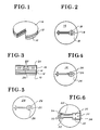
- FIG. 1 there is shown a perspective view, partly in section, of a wafer that is used for the formation of a flexible microcircuit in accordance with the present invention.
- the overall wafer comprises a base wafer 10, preferably of silicon, which is readily commercially available and is typically approximately 2 inches in diameter and about 10 mils thick.
- Such commercial wafers 10 can be purchased preferably having one side polished, the other side may, but need not, be polished.
- the base wafer 10 may be of materials other than silicon that are not attacked by the various etching steps employed herein and which preferably have at least one smooth surface. As described herein, only one flexible microcircuit is illustrated on base wafer 10 for clarity, however, in practice, a plurality are formed on a typical 2 inch diameter wafer.
- a silver coating 12 is vacuum evaporated by conventional techniques on to the base wafer 10.
- the silver coating 12 is approximately 1 micron in thickness and the silver is coated on to the polished side of base wafer 10.
- a polyimide layer 14 On to the silver coating 12, is applied a polyimide layer 14.
- Various techniques may be employed to apply the polyimide layer 14 however, the preferred technique is to spin coat the polyimide in a commercial spin coating machine, one of which that is suitable is Model EO-101 photoresist spinner available from Headway Research of Garland, Texas.
- the wafer In applying the polyimide layer 14 with a spin coater, the wafer is placed on a spinner in the spin coater with the silver coating 12 facing upwardly.
- Base polyimide material itself is commercially available as a thick, syrup-like liquid, one of such commercial suppliers is E. I. Du Pont De Nemours & Company.
- the silver coating 12 is flooded with polyimide and then spun at approximately 4000 rpm for about 30 seconds in order to form a polyimide layer 14 of about 35 micrometers.
- the polyimide material is cured by heating, a typical heating cycle comprises an oven bake at about 80°C for fifteen minutes followed by setting the wafer on a hot plate and increasing the temperature in discrete steps up to 300°F in about 1/2 hour, all of which should be handled in a dust-free atmosphere.
- the precise curing of the polyimide may be done in various heating steps, by oven heating alone or by heating on the hot plate alone. Generally, instructions on the amount cure necessary are provided by the manufacturers of the particular polyimide utilized.
- the final wafer has a fully cured polyimide layer 14 of about 35 microns uniformly distributed atop the silver coating 12.
- a series of steps is commenced utilizing photoresist techniques to form the flexible microcircuit.
- a photoresist material one of which that may be used is a material identified as AZ-1350-J supplied commercially by Shipley Company of Newton, Massachusetts is spun on, to the completed wafer with the cured polyimide layer 14. That material is spin coated at about 4000 rpm for a time of between about 10 to about 30 seconds. The photoresist is thereafter semi-cured by baking for about five minutes at 60°C in a dust free atmosphere.
- the photoresist material 16 now covering the entire polyimide layer 14 is thereafter exposed to light under a mask.
- the mask is designed such that light does not recall the photoresist except in certain surface areas. As shown in FIG. 2, only the areas 18 receive the light.
- the light is ultraviolet light, by using a mercury arc lamp and exposure is for about 1.5 minutes; overall energy expended for each exposure is approximately 360 millijoules.
- the wafer is soaked in chlorobenzine for about five minutes.
- the chlorobenzine soaks into the top surface of the photoresist material 16 that is not completely cured and decreases the solubility of the photoresist material to a developer in those areas 18 that were not exposed to the light that is, the surface areas 18 become less soluble to the later used developer.
- the wafer After the chlorobenzine soak, the wafer is drained and the developing step takes place.
- the wafer is immersed in AZ developer at room temperature for approximately twice as long as the suppliers normal recommended developing time to account for the chlorobenzine soak.
- FIG. 3 an enlarged cross sectional view of one of the areas 18 is shown and the effect of the chlorobenzine soak can be seen.
- the base wafer 10 upon which is the silver coating 12 and the cured polyimide layer 14.
- the photoresist material 16 has been eaten away by the developer to form over hangs 20 in photoresist material 16 by the developer having removed more of the photoresist material 16 at the areas shown as 22.
- chlorobenzine caused the less soluble surface area of the photoresist material 16 in areas 18 to resist the ending effect of the developer and, thus, more erosion takes place in the areas 22 beneath the surface of overhangs 20.
- the completion of the developing step can be ascertained visibly and the wafer removed from the developer.
- the wafer is thereafter rinsed in deionized water and blown dry.
- the entire wafer is coated with aluminum in a vacuum chamber by conventional evaporation techniques.
- the aluminum coating 24 is approximately 1 micron in thickness and in the space where the photoresist material 16 has been removed an aluminum run 26 is formed by the evaporated aluminum passing through the overhangs 20. It is important to note that the lift off technique has left very little surface of the overhangs 20 on which the evaporized aluminum can become attached, thus, the overhangs 20 as well as the areas 22 do not become coated with aluminum, the reason for which will become apparent in the next step.
- the aluminum run 26 is thus deposited directly upon the polyimide layer 14 and is in the configuration of the areas 18, referring back to FIG. 2.
- Photoresist remover is next utilized in order to remove the photoresist material 16, and, with it, the aluminum coating 24, leaving only the aluminum runs 26.
- photoresist remover one type of which is Shipley plate resist remover, commercially available, preferably in an ultrasonic bed so that the photoresist material 16 is completely removed.
- FIG. 4 that is, a wafer wherein the top surface is almost entirely the polyimide layer 14 upon which are formed, the aluminum runs 26.
- the subsequent steps involve forming holes of approximately 2 mils in diameter through the aluminum runs 26.
- FIG. 5 there is shown the wafer which has now been entirely plated by a chrome layer 28 by RF sputtering or comparable means with chromium of a thickness in the range of about 2000-5000 angstrom.
- a photoresist is spin coated on to the chrome layer 28 in the manner as previously explained and partially cured.
- a mask is put over the wafer that covers all of the wafer except for the minute holes 30, a small boundary 32 surrounding the periphery of the eventual microcircuit, and areas 34 at each end of the microcircuit configuration, thus it is those areas where removal of the chromium is desired. Accordingly, again using the previously explained photoresist techniques,upon developing step any photoresist is removed from the area of the holes 30, the boundary 32 and the outer areas 34.
- the outline of the eventual microcircuit is shown where the outside areas 34 ⁇ are chromium, the boundaries 32 ⁇ are chromium and the area 30 ⁇ with in holes are chromium, the remaining area 36 is all covered by the photoresist material.
- the wafer is then dipped in a conventional chromium etch where the chromium is removed.
- the wafer is merely dipped at room temperature in the chrome etch and visually observed that the chromium is completely removed.
- a typical chromium etch many of which are suitable and some of which use ceric ammonium nitrate.
- the wafer after immersion in the chrome etch, takes on the appearance of FIG. 8 wherein the surface showing within the holes 30 ⁇ is the aluminum from aluminum runs 26, the outside areas 34 ⁇ now are polyimide, the boundaries 32 ⁇ are also polyimide and the remaining area of the wafer is covered by the photoresist surface 36.
- the wafer After washing in deionized water and according to previously described procedures, the wafer is immersed in an aluminum etch, one of which is polyphosphoric acid at about 90° C for about 10 seconds to remove the aluminum surface within the holes 30 ⁇ . The removal of that aluminum can be visually perceived and the wafer rinsed and blow dried.
- an aluminum etch one of which is polyphosphoric acid at about 90° C for about 10 seconds to remove the aluminum surface within the holes 30 ⁇ . The removal of that aluminum can be visually perceived and the wafer rinsed and blow dried.
- the wafer is almost the same as FIG. 8, when the end areas 34 ⁇ and boundary area 32 ⁇ are still polyimide surfaces, the overall area 36 is photoresist material but the holes 30 ⁇ are now also down to the polyimide layer (all of the polyimide layers are the polyimide layer 14 of FIG. 1).
- the wafer is then subjected to photoresist remover and which removes all of the photoresist material 36 leaving, as shown in FIG. 10, the surface 36 ⁇ as chromium, the remaining areas, 30 ⁇ , 32 ⁇ , 34 ⁇ down to the polyimide material 14 (FIG. 1). Again, the wafer is rinsed in water and blown dry.
- a polyimide etch next takes place in a vacuum system and when oxygen is leaked back into the system and which acts to erode the polyimide at a faster rate than the metals. Accordingly, the polyimide surface is reduced by erosion.
- the wafer is again dipped into a chrome etch at room temperature, and the etch maybe the same as previously described.
- the chrome etch removes the top surface 36 ⁇ (FIG 10) on top of the microcircuit, thereby exposing the aluminum runs 26 (not shown in FIG 10) and which etch also eats through the underlying silver coating 12 (not shown in FIG. 10). Accordingly, the microcircuit is eventually undercut by the etch and it lifts off the surface of the wafer.
- the flexible microcircuit is a polyimide base 38; having thereon, conductive aluminum runs 40 including contact areas 42, one end of which has holes approximately 16 mils in diameter and is sufficiently large for hard wiring to electronic apparatus and the other end has holes approximately 2 mils in diameter and is suitable for attaching a microchip.
Landscapes
- Engineering & Computer Science (AREA)
- Manufacturing & Machinery (AREA)
- Microelectronics & Electronic Packaging (AREA)
- Chemical & Material Sciences (AREA)
- Chemical Kinetics & Catalysis (AREA)
- General Chemical & Material Sciences (AREA)
- Internal Circuitry In Semiconductor Integrated Circuit Devices (AREA)
- Parts Printed On Printed Circuit Boards (AREA)
- Materials For Medical Uses (AREA)
Abstract
Description
- This invention relates to a method of producing a flexible microcircuit having conductive paths or runs for connection between a device such as a semiconductor and a connector for joining with hard wiring.
- There are many methods of fabricating flexible microcircuits and which include processing steps with photoresist methods to produce conductive runs therein. Many, however, are not optimized or are used with larger flexible circuits that can be more easily produced in commercial quantities.
- In particular, it has been difficult to fabricate a flexible microcircuit of the size usable in attaching a distal end thereof to a semiconductor device, such as a JFET or ISFET to produce a freely suspended device on the end of the flexible microcircuit. The flexible microcircuit for such use must be specifically manufactured and must have, at its distal ends extremely minute holes for providing connection with the semiconductor device.
- An example of such a semiconductor device is in United States Patent 4,180,771 of Guckel et al. Such devices are capable of being introduced into a person's blood stream for in vivo measurements of pH etc., therefore, must be extremely minute as well as flexible so that the semiconductor device, as well as the flexible circuit holding that device can enter the patient's blood stream without creating a hazardous interference with the natural flow of blood therein.
- The distal end of such a flexible microcircuit to be connected to the JFET must have a plurality of holes having diameters of about .002" in order to be connectible thereto, and the proximal end thereof adaptable for connection to hard wiring devices.
- Because of the size of the microcircuit itself and the requirement for extremely minute yet accurately positioned holes, the fabrication of such microcircuit is difficult.
- It is an aim of the present invention to provide a method of producing a flexible microcircuit that can be used to produce a circuit that can be utilized for freely suspending a semiconductor device or chip on the distal end and which is sufficiently minute so as to be introducible into the blood stream of a living patient. The method produces a flexible microcircuit having holes at its distal end of about .002 inches in diameter and has conductive runs for providing electrical connection from the distal end to the proximal end where hard wire connections can be accomplished.
- According to the present invention, a method of making a flexible microcircuit having conductive runs is characterised by the steps of:
- a. coating base polyimide material on to a substrate,
- b. creating a photoresist mask surface on the base polyimide in all areas except where conductive runs are desired,
- c. coating aluminum over the entire polyimide surface,
- d. removing the photoresist mask surface to remove the aluminum coating in all areas but the desired aluminum runs on the polyimide surface,
- e. coating the entire polyimide surface and aluminum runs with chromium,
- f. creating a photoresist mask surface of predetermined shape on the chromium surface outlining the desired form of the flexible microcircuit and desired holes in the aluminum runs,
- g. removing the chromium in the areas outlining the microcircuit and at the desired holes to be formed in the aluminum runs, thereby exposing a portion of the aluminum runs in the shape of the desired holes,
- h. removing the exposed aluminum in the shape of the desired holes, thereby exposing the polyimide material in the shape of the desired holes,
- i. removing the exposed polyimide to create the desired holes through the polyimide,
- j. removing the chrome surface to thus remove the polyimide microcircuit from the substrate.
- The method comprises coating base polyimide material onto a silver coated silicon substrate to a predetermined thickness. The polyimide is thus the main composition of the flexible microcircuit and on which the conductive runs are formed. By photographic techniques and masking, a photoresist surface is created on the base polyimide everywhere on that surface where no subsequent metallic surfaces are desired, i.e. the conductive runs and contact areas. A coating of aluminum is thereafter applied to a predetermined thickness to the entire polyimide surface by evaporation.
- Next, the photoresist is dissolved and, therefore, removes all of the aluminum coated surface covering the photoresist, that is, all of the polyimide surface where metallic surfaces are not desired. Upon removal of such surface area the remaining aluminum coating on the polyimide surface is in the form of the desired conductive runs and surfaces for connections.
- A thin layer of chromium is then deposited to a predetermined thickness over the entire surface of the polyimide material thus coating both the conductive area (runs) and the nonmetallic surface area.
- Another photoresist mask surface is applied to the surface of the chromium; this time the mask surface is applied to form the pattern of the desired holes in the conductive runs and to form the outside pattern of the flexible microcircuit itself; that is, the mask area is created in the shape of tiny holes for later use in applying the semiconductor device to the distal end and for hard wire connection to the proximal end. Also, the mask surrounds the external desired shape of the end product flexible microcircuit.
- The chrome surface is thereafter etched away, due to the photoresist mask, such that only those areas where the mask has been formed are effected by the etch. Thus, the tiny holes are etched down to the aluminum coating and the overall shape is formed by the etch eroding the chromium surrounding the periphery of the desired final shape down to the polyimide.
- The aluminum is then etched away, therefore, the area where the holes are desired are removed. As such, therefore, those areas where the aluminum has been removed expose the base polyimide material.
- The polyimide in those exposed areas is thereafter removed by an oxygen plasma etch thus completing formation of the holes in the flexible microcircuit and removing the surrounding polyimide in order to leave polyimide in the desired shape still affixed to the silver coated silicon substrate.
- The entire unit is then chrome etched and which removes the chrome mask and also attacks the silver surface such that microcircuit frees from the silicon substrate and the final flexible microcircuit is thus completed and whichcomprises a polyimide base material upon which are formed aluminum runs with minute accurate holes for connections at the distal and proximal ends. The techniques of the present invention can readily be used to produce a microcircuit approximately 1-2 mils thick less than 20 mils in width, and about 2.5 inches in length.
- An embodiment of the invention will now be described, by way of example, reference being made to the Figures of the accompanying diagrammatic drawings in which:-
- FIG. 1 is a perspective view, partially cut away, of a typical wafer on which the microcircuit of the present invention is formed;
- FIG. 2 is a plan view of the wafer of FIG. 1 illustrating one of the steps of the invention;
- FIG. 3 is an enlarged cross sectional view illustrating one of the steps of the invention
- FIG. 4 - 10 are further plan views illustrating further sequential steps in carrying out the invention; and
- FIG. 11 is a perspective view of a completed microcircuit produced by carrying out the invention process.
- In FIG. 1, there is shown a perspective view, partly in section, of a wafer that is used for the formation of a flexible microcircuit in accordance with the present invention. As shown, the overall wafer comprises a
base wafer 10, preferably of silicon, which is readily commercially available and is typically approximately 2 inches in diameter and about 10 mils thick. Suchcommercial wafers 10 can be purchased preferably having one side polished, the other side may, but need not, be polished. - The
base wafer 10 may be of materials other than silicon that are not attacked by the various etching steps employed herein and which preferably have at least one smooth surface. As described herein, only one flexible microcircuit is illustrated onbase wafer 10 for clarity, however, in practice, a plurality are formed on a typical 2 inch diameter wafer. - To prepare the
base wafer 10 for the further steps of the invention, asilver coating 12 is vacuum evaporated by conventional techniques on to thebase wafer 10. - The
silver coating 12 is approximately 1 micron in thickness and the silver is coated on to the polished side ofbase wafer 10. - On to the
silver coating 12, is applied apolyimide layer 14. Various techniques may be employed to apply thepolyimide layer 14 however, the preferred technique is to spin coat the polyimide in a commercial spin coating machine, one of which that is suitable is Model EO-101 photoresist spinner available from Headway Research of Garland, Texas. In applying thepolyimide layer 14 with a spin coater, the wafer is placed on a spinner in the spin coater with thesilver coating 12 facing upwardly. - Base polyimide material itself is commercially available as a thick, syrup-like liquid, one of such commercial suppliers is E. I. Du Pont De Nemours & Company. The
silver coating 12 is flooded with polyimide and then spun at approximately 4000 rpm for about 30 seconds in order to form apolyimide layer 14 of about 35 micrometers. After coating, the polyimide material is cured by heating, a typical heating cycle comprises an oven bake at about 80°C for fifteen minutes followed by setting the wafer on a hot plate and increasing the temperature in discrete steps up to 300°F in about 1/2 hour, all of which should be handled in a dust-free atmosphere. - The precise curing of the polyimide may be done in various heating steps, by oven heating alone or by heating on the hot plate alone. Generally, instructions on the amount cure necessary are provided by the manufacturers of the particular polyimide utilized.
- The final wafer has a fully cured
polyimide layer 14 of about 35 microns uniformly distributed atop thesilver coating 12. - Turning now to FIG. 2, a series of steps is commenced utilizing photoresist techniques to form the flexible microcircuit. Next, a photoresist material, one of which that may be used is a material identified as AZ-1350-J supplied commercially by Shipley Company of Newton, Massachusetts is spun on, to the completed wafer with the cured
polyimide layer 14. That material is spin coated at about 4000 rpm for a time of between about 10 to about 30 seconds. The photoresist is thereafter semi-cured by baking for about five minutes at 60°C in a dust free atmosphere. - The
photoresist material 16 now covering theentire polyimide layer 14 is thereafter exposed to light under a mask. The mask is designed such that light does not recall the photoresist except in certain surface areas. As shown in FIG. 2, only theareas 18 receive the light. Typically, the light is ultraviolet light, by using a mercury arc lamp and exposure is for about 1.5 minutes; overall energy expended for each exposure is approximately 360 millijoules. - As will be later explained, the photoresist covering those
areas 18 that are subject to the light are eventually developed away, but a technique known as "lift-off" is utilized prior to the actual development. - The wafer is soaked in chlorobenzine for about five minutes. The chlorobenzine soaks into the top surface of the
photoresist material 16 that is not completely cured and decreases the solubility of the photoresist material to a developer in thoseareas 18 that were not exposed to the light that is, thesurface areas 18 become less soluble to the later used developer. - After the chlorobenzine soak, the wafer is drained and the developing step takes place. The wafer is immersed in AZ developer at room temperature for approximately twice as long as the suppliers normal recommended developing time to account for the chlorobenzine soak.
- Turning now to FIG. 3, an enlarged cross sectional view of one of the
areas 18 is shown and the effect of the chlorobenzine soak can be seen. In FIG. 3, there is shown, thebase wafer 10 upon which is thesilver coating 12 and the curedpolyimide layer 14. - The
photoresist material 16 has been eaten away by the developer to form over hangs 20 inphotoresist material 16 by the developer having removed more of thephotoresist material 16 at the areas shown as 22. As explained, the use of chlorobenzine caused the less soluble surface area of thephotoresist material 16 inareas 18 to resist the ending effect of the developer and, thus, more erosion takes place in theareas 22 beneath the surface ofoverhangs 20. - The completion of the developing step can be ascertained visibly and the wafer removed from the developer. The wafer is thereafter rinsed in deionized water and blown dry.
- As the next step, the entire wafer is coated with aluminum in a vacuum chamber by conventional evaporation techniques. In FIG. 3, the
aluminum coating 24 is approximately 1 micron in thickness and in the space where thephotoresist material 16 has been removed analuminum run 26 is formed by the evaporated aluminum passing through theoverhangs 20. It is important to note that the lift off technique has left very little surface of theoverhangs 20 on which the evaporized aluminum can become attached, thus, theoverhangs 20 as well as theareas 22 do not become coated with aluminum, the reason for which will become apparent in the next step. - The
aluminum run 26 is thus deposited directly upon thepolyimide layer 14 and is in the configuration of theareas 18, referring back to FIG. 2. - Photoresist remover is next utilized in order to remove the
photoresist material 16, and, with it, thealuminum coating 24, leaving only the aluminum runs 26. - To effect photoresist removal, the wafer is immersed in photoresist remover, one type of which is Shipley plate resist remover, commercially available, preferably in an ultrasonic bed so that the
photoresist material 16 is completely removed. The result is shown in FIG. 4, that is, a wafer wherein the top surface is almost entirely thepolyimide layer 14 upon which are formed, the aluminum runs 26. - The subsequent steps involve forming holes of approximately 2 mils in diameter through the aluminum runs 26.
- In FIG. 5, there is shown the wafer which has now been entirely plated by a
chrome layer 28 by RF sputtering or comparable means with chromium of a thickness in the range of about 2000-5000 angstrom. - Again, a photoresist is spin coated on to the
chrome layer 28 in the manner as previously explained and partially cured. A mask is put over the wafer that covers all of the wafer except for the minute holes 30, asmall boundary 32 surrounding the periphery of the eventual microcircuit, andareas 34 at each end of the microcircuit configuration, thus it is those areas where removal of the chromium is desired. Accordingly, again using the previously explained photoresist techniques,upon developing step any photoresist is removed from the area of theholes 30, theboundary 32 and theouter areas 34. - Accordingly, as now seen in FIG.7, the outline of the eventual microcircuit is shown where the outside areas 34ʹ are chromium, the boundaries 32ʹ are chromium and the area 30ʹ with in holes are chromium, the remaining
area 36 is all covered by the photoresist material. - The wafer is then dipped in a conventional chromium etch where the chromium is removed. The wafer is merely dipped at room temperature in the chrome etch and visually observed that the chromium is completely removed. A typical chromium etch, many of which are suitable and some of which use ceric ammonium nitrate.
- The wafer, after immersion in the chrome etch, takes on the appearance of FIG. 8 wherein the surface showing within the holes 30ʺ is the aluminum from aluminum runs 26, the outside areas 34ʺ now are polyimide, the boundaries 32ʺ are also polyimide and the remaining area of the wafer is covered by the
photoresist surface 36. - After washing in deionized water and according to previously described procedures, the wafer is immersed in an aluminum etch, one of which is polyphosphoric acid at about 90° C for about 10 seconds to remove the aluminum surface within the holes 30ʺ. The removal of that aluminum can be visually perceived and the wafer rinsed and blow dried.
- At this point, in FIG. 9, the wafer is almost the same as FIG. 8, when the end areas 34ʺ and boundary area 32ʺ are still polyimide surfaces, the
overall area 36 is photoresist material but the holes 30ʹ are now also down to the polyimide layer (all of the polyimide layers are thepolyimide layer 14 of FIG. 1). - The wafer is then subjected to photoresist remover and which removes all of the
photoresist material 36 leaving, as shown in FIG. 10, the surface 36ʹas chromium, the remaining areas, 30ʺ, 32ʺ, 34ʺ down to the polyimide material 14 (FIG. 1). Again, the wafer is rinsed in water and blown dry. - A polyimide etch next takes place in a vacuum system and when oxygen is leaked back into the system and which acts to erode the polyimide at a faster rate than the metals. Accordingly, the polyimide surface is reduced by erosion.
- Finally, the wafer is again dipped into a chrome etch at room temperature, and the etch maybe the same as previously described. The chrome etch removes the top surface 36ʹ (FIG 10) on top of the microcircuit, thereby exposing the aluminum runs 26 (not shown in FIG 10) and which etch also eats through the underlying silver coating 12 (not shown in FIG. 10). Accordingly, the microcircuit is eventually undercut by the etch and it lifts off the surface of the wafer.
- As shown in FIG 11, therefore, the flexible microcircuit is a
polyimide base 38; having thereon, conductive aluminum runs 40 includingcontact areas 42, one end of which has holes approximately 16 mils in diameter and is sufficiently large for hard wiring to electronic apparatus and the other end has holes approximately 2 mils in diameter and is suitable for attaching a microchip.
Claims (6)
Applications Claiming Priority (2)
| Application Number | Priority Date | Filing Date | Title |
|---|---|---|---|
| US892514 | 1986-08-04 | ||
| US06/892,514 US4711791A (en) | 1986-08-04 | 1986-08-04 | Method of making a flexible microcircuit |
Publications (2)
| Publication Number | Publication Date |
|---|---|
| EP0257801A2 true EP0257801A2 (en) | 1988-03-02 |
| EP0257801A3 EP0257801A3 (en) | 1988-07-06 |
Family
ID=25400047
Family Applications (1)
| Application Number | Title | Priority Date | Filing Date |
|---|---|---|---|
| EP87306561A Withdrawn EP0257801A3 (en) | 1986-08-04 | 1987-07-24 | Method of making a flexible microcircuit |
Country Status (4)
| Country | Link |
|---|---|
| US (1) | US4711791A (en) |
| EP (1) | EP0257801A3 (en) |
| JP (1) | JPS6392102A (en) |
| CA (1) | CA1271268A (en) |
Cited By (3)
| Publication number | Priority date | Publication date | Assignee | Title |
|---|---|---|---|---|
| WO1997006656A3 (en) * | 1995-08-09 | 1997-03-27 | Philips Electronics Nv | Method of manufacturing devices comprising a base with a conductor pattern of electrical conductors |
| US7481771B2 (en) | 2002-01-22 | 2009-01-27 | Cardiomems, Inc. | Implantable wireless sensor for pressure measurement within the heart |
| US7699059B2 (en) | 2002-01-22 | 2010-04-20 | Cardiomems, Inc. | Implantable wireless sensor |
Families Citing this family (4)
| Publication number | Priority date | Publication date | Assignee | Title |
|---|---|---|---|---|
| GB9401869D0 (en) * | 1994-02-01 | 1994-03-30 | Heinze Dyconex Patente | Improvements in and relating to printed circuit boards |
| US6218628B1 (en) | 1994-05-18 | 2001-04-17 | Dyconex Patente Ag | Foil circuit boards and semifinished products and method for the manufacture thereof |
| US6391220B1 (en) | 1999-08-18 | 2002-05-21 | Fujitsu Limited, Inc. | Methods for fabricating flexible circuit structures |
| US20060222846A1 (en) * | 2005-04-01 | 2006-10-05 | General Electric Company | Reflective and resistant coatings and methods for applying to composite structures |
Family Cites Families (12)
| Publication number | Priority date | Publication date | Assignee | Title |
|---|---|---|---|---|
| DE2260958A1 (en) * | 1972-12-13 | 1974-06-27 | Fortin Laminating Corp | Metal faced laminate - for making printed circuits |
| US3881884A (en) * | 1973-10-12 | 1975-05-06 | Ibm | Method for the formation of corrosion resistant electronic interconnections |
| DE2432719B2 (en) * | 1974-07-08 | 1977-06-02 | Siemens AG, 1000 Berlin und 8000 München | PROCESS FOR CREATING FINE STRUCTURES FROM VAPORIZABLE MATERIALS ON A BASE AND APPLYING THE PROCESS |
| DE2638799C3 (en) * | 1976-08-27 | 1981-12-03 | Ibm Deutschland Gmbh, 7000 Stuttgart | Process for improving the adhesion of metallic conductor tracks to polyimide layers in integrated circuits |
| US4246595A (en) * | 1977-03-08 | 1981-01-20 | Matsushita Electric Industrial Co., Ltd. | Electronics circuit device and method of making the same |
| US4180771A (en) * | 1977-12-02 | 1979-12-25 | Airco, Inc. | Chemical-sensitive field-effect transistor |
| US4200668A (en) * | 1978-09-05 | 1980-04-29 | Western Electric Company, Inc. | Method of repairing a defective photomask |
| US4508813A (en) * | 1980-06-16 | 1985-04-02 | Fujitsu Limited | Method for producing negative resist images |
| US4339305A (en) * | 1981-02-05 | 1982-07-13 | Rockwell International Corporation | Planar circuit fabrication by plating and liftoff |
| US4563407A (en) * | 1982-11-16 | 1986-01-07 | Hoya Corporation | Photo-mask blank comprising a shading layer having a variable etch rate |
| US4480288A (en) * | 1982-12-27 | 1984-10-30 | International Business Machines Corporation | Multi-layer flexible film module |
| GB2138025B (en) * | 1983-04-13 | 1986-09-24 | Furukawa Electric Co Ltd | Silver-coated electric materials and a method for their production |
-
1986
- 1986-08-04 US US06/892,514 patent/US4711791A/en not_active Expired - Fee Related
-
1987
- 1987-07-02 CA CA000541112A patent/CA1271268A/en not_active Expired
- 1987-07-24 EP EP87306561A patent/EP0257801A3/en not_active Withdrawn
- 1987-08-03 JP JP62194284A patent/JPS6392102A/en active Pending
Cited By (3)
| Publication number | Priority date | Publication date | Assignee | Title |
|---|---|---|---|---|
| WO1997006656A3 (en) * | 1995-08-09 | 1997-03-27 | Philips Electronics Nv | Method of manufacturing devices comprising a base with a conductor pattern of electrical conductors |
| US7481771B2 (en) | 2002-01-22 | 2009-01-27 | Cardiomems, Inc. | Implantable wireless sensor for pressure measurement within the heart |
| US7699059B2 (en) | 2002-01-22 | 2010-04-20 | Cardiomems, Inc. | Implantable wireless sensor |
Also Published As
| Publication number | Publication date |
|---|---|
| CA1271268A (en) | 1990-07-03 |
| JPS6392102A (en) | 1988-04-22 |
| US4711791A (en) | 1987-12-08 |
| EP0257801A3 (en) | 1988-07-06 |
Similar Documents
| Publication | Publication Date | Title |
|---|---|---|
| JP3135930B2 (en) | Thin film electrical equipment | |
| US5907791A (en) | Method of making semiconductor devices by patterning a wafer having a non-planar surface | |
| JP2951215B2 (en) | Method of manufacturing fine pattern electronic interconnect structure by phase mask laser | |
| US4711791A (en) | Method of making a flexible microcircuit | |
| US5503961A (en) | Process for forming multilayer lift-off structures | |
| US4139434A (en) | Method of making circuitry with bump contacts | |
| CN114613584A (en) | Etching method for soft magnetic material and soft magnetic strip | |
| JPS63132452A (en) | Pattern forming method | |
| JP3140369B2 (en) | Method of forming electrode pattern at deep groove bottom | |
| US3951659A (en) | Method for resist coating of a glass substrate | |
| CN114906798B (en) | Method for growing copper pillars on the surface of packaging substrate based on MEMS processing technology | |
| JP3726578B2 (en) | Manufacturing method of semiconductor device | |
| GB2234365A (en) | Strain gauge encapsulation process | |
| JPH11219986A (en) | Method for manufacturing TAB tape carrier | |
| KR0161120B1 (en) | Pattern for confirming adhesion of photoresist in semiconductor apparatus | |
| US5891749A (en) | Process for forming photoresist pattern in semiconductor device | |
| JPS604221A (en) | Manufacture of semiconductor device | |
| JPS6273744A (en) | Forming method for metal wiring pattern | |
| JPH04324445A (en) | Mask for exposing and production thereof | |
| JPH0552076B2 (en) | ||
| JPS6232617A (en) | Semiconductor device and its manufacture | |
| JPS59155934A (en) | Forming method of minute pattern | |
| KR930014853A (en) | How to Form Wire Bonding Pads | |
| JP2589471B2 (en) | Method for manufacturing semiconductor device | |
| KR100248328B1 (en) | Manufacturing Method of Semiconductor Acceleration Sensor |
Legal Events
| Date | Code | Title | Description |
|---|---|---|---|
| PUAI | Public reference made under article 153(3) epc to a published international application that has entered the european phase |
Free format text: ORIGINAL CODE: 0009012 |
|
| AK | Designated contracting states |
Kind code of ref document: A2 Designated state(s): AT BE CH DE ES FR GB GR IT LI LU NL SE |
|
| PUAL | Search report despatched |
Free format text: ORIGINAL CODE: 0009013 |
|
| AK | Designated contracting states |
Kind code of ref document: A3 Designated state(s): AT BE CH DE ES FR GB GR IT LI LU NL SE |
|
| 17P | Request for examination filed |
Effective date: 19881012 |
|
| STAA | Information on the status of an ep patent application or granted ep patent |
Free format text: STATUS: THE APPLICATION IS DEEMED TO BE WITHDRAWN |
|
| 18D | Application deemed to be withdrawn |
Effective date: 19910202 |
|
| RIN1 | Information on inventor provided before grant (corrected) |
Inventor name: WISEMAN, CHARLES D. Inventor name: THEISEN, WILLIAM M. |